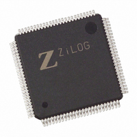
Z8018233ASG Zilog, Z8018233ASG Datasheet - Page 61

Z8018233ASG
Manufacturer Part Number
Z8018233ASG
Description
IC 33MHZ STATIC MIMIC 100-LQFP
Manufacturer
Zilog
Datasheet
1.Z8018233FSG.pdf
(109 pages)
Specifications of Z8018233ASG
Processor Type
Z180
Features
Smart Peripheral Controller
Speed
33MHz
Voltage
5V
Mounting Type
Surface Mount
Package / Case
100-LQFP
Processor Series
Z8018xx
Core
Z80
Data Bus Width
8 bit
Program Memory Type
ROMLess
Interface Type
UART
Maximum Clock Frequency
33 MHz
Number Of Programmable I/os
24
Number Of Timers
2
Operating Supply Voltage
4.5 V to 5.5 V
Maximum Operating Temperature
+ 70 C
Mounting Style
SMD/SMT
Minimum Operating Temperature
0 C
Lead Free Status / RoHS Status
Lead free / RoHS Compliant
Available stocks
Company
Part Number
Manufacturer
Quantity
Price
INTERRUPT EDGE/PIN MUX REGISTER
Bits 7-6. These bits control the interrupt capture logic for
the external /INT2 PIN. When programmed as ‘0X’, the
/INT2 pin performs as the normal level detecting interrupt
pin. When programmed as 10 the negative edge detection
is enabled. Any falling edge latches an active Low on the
internal /INT2 of the Z180. This interrupt must be cleared by
writing a 1 to bit 7 of the Port C Data Register. Programming
these control bits to 11 enables rising edge interrupts to be
latched. The latch is cleared in the same fashion as the
falling edge.
Bits 5-4. These bits control the interrupt capture logic for
the external /INT1 PIN. When programmed as ‘0X’, the
/INT1 pin performs as the normal level detecting interrupt
pin. When programmed as 10, the negative edge detection
is enabled. Any falling edge latches an active Low on the
internal /INT1 of the Z180. This interrupt must be cleared by
writing a 1 to bit 6 of the Port C Data Register. Programming
these control bits to 11 enables rising edge interrupts to be
latched. The latch is cleared in the same fashion as the
falling edge. Edge detect logic cannot be used in Emulation
Adaptor EV mode 1.
Bit 3. Programming this bit to 1 selects the /MRD and the
/MWR functions. The default for power up and /RESET
conditions is 1, i.e., the /MRD and /MWR. By programming
DS971820600
Zilog
D7 D6 D5 D4 D3 D2 D1
0
1
Figure 59. Interrupt Edge/Pin MUX Register
0
(Z180 MPU Read/Write, Address xxDFH)
1
P R E L I M I N A R Y
1
PS009801-0301
1
0
D0
0
this bit to 0 the /MREQ Z180 function is enabled, as well as
the PC2//RTSA function on the PC2//RTSA//MWR pin. If the
/MREQ Z180 function is enabled, any external bus master
must be prevented from asserting Z182's IRD signal unless
accessing Z182's IO.
Bit 2. This bit selects the /IOCS function which is the default
for power up and /RESET conditions. By programming this
bit to 0 the IEO function is enabled for this multiplexed pin.
Bit 1. This bit selects the low noise or normal drive feature
for the Z182 pins . The default at power up is normal drive
for Z182 pins. By programming this bit to 1, low noise for
the Z182 pins is chosen and the output drive capability of
the following pins is reduced to 25% of the original drive
capability:
Programming this bit to 0 selects normal drive for the Z182
pins. Refer to the Z8S180 Product Specification for Low
noise control of Z180 pins.
Halt Recovery Select
1 16 Cycle delay on Halt recovery
0 No wait delay on Halt recovery
Low Noise Select
1 Select low noise for Z182(not Z180)
0 Select normal drive for Z182 pins
IEO,/IOCS Select
1 Select/IOCS Function
0 Select IEO Function
/MREQ, /MRD, PC2, /RTSA, /MWR Select
1 Select /MRD, /MWR
0 Select /MREQ, PC2, /RTSA
/INT1 Mode Select
0X Normal Level Detect
10 Falling (Neg) Edge Det
11 Rising (Pos) Edge Det
/INT2 Mode Select
0X Normal Level Detect
10 Falling (Neg) Edge Det
11 Rising (Pos) Edge Det
- CKS
- RxS/CTS1
- TxS
- CKA1/TEND0
- TxA1
Z
ILOG
I
NTELLIGENT
- CKA0/DREQ0
- TxA0
Z80182/Z8L182
P
ERIPHERAL
3-61


