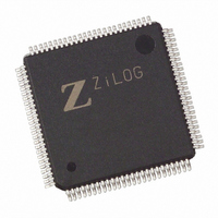
Z8018233ASG Zilog, Z8018233ASG Datasheet - Page 62

Z8018233ASG
Manufacturer Part Number
Z8018233ASG
Description
IC 33MHZ STATIC MIMIC 100-LQFP
Manufacturer
Zilog
Datasheet
1.Z8018233FSG.pdf
(109 pages)
Specifications of Z8018233ASG
Processor Type
Z180
Features
Smart Peripheral Controller
Speed
33MHz
Voltage
5V
Mounting Type
Surface Mount
Package / Case
100-LQFP
Processor Series
Z8018xx
Core
Z80
Data Bus Width
8 bit
Program Memory Type
ROMLess
Interface Type
UART
Maximum Clock Frequency
33 MHz
Number Of Programmable I/os
24
Number Of Timers
2
Operating Supply Voltage
4.5 V to 5.5 V
Maximum Operating Temperature
+ 70 C
Mounting Style
SMD/SMT
Minimum Operating Temperature
0 C
Lead Free Status / RoHS Status
Lead free / RoHS Compliant
Available stocks
Company
Part Number
Manufacturer
Quantity
Price
Zilog
INTERRUPT EDGE/PIN MUX REGISTER (Continued)
Bit 0. Programming this bit to 1 selects a 16 cycle wait
delay on recovery from HALT. Halt Recovery is disabled if
bit 5 of the enhancement register is set to 1. A 0 selects no
wait delay on Halt recovery.
If Halt Recovery is selected, the following pins assume the
following states during halt and during the recovery, whether
it is in HALT, SLP, IDLE or STBY Modes:
3-62
MREQ/MRD
Data Bus
BUSACK
Address
RFSH
IORQ
IOCS
MWR
WR
RD
M1
ST
E
= Z
= Z
= Z
= Z
= Z
= 1
= 1
= 1
= 1
= 1
= Note 3
= Z
= 1 (Note 4)
P R E L I M I N A R Y
PS009801-0301
Notes:
1. This assumes that BUSREQ is not activated during the
2. This assumes that the refresh is not enabled. This would
3. There is no control on the E line during the halt recovery
4. This is only true if MWR function is enabled.
The Halt recovery mode is implemented by applying wait
states to the next CPU operation following the exit from
halt. All signals listed above are forced to their specified
state (unless otherwise noted) during halt and also during
the recovery state. Sixteen cycles after the halt pin goes
High the signals are released to their normal state, then
eight wait states are inserted to allow proper access to
accommodate slow memories.
After the first memory access, the wait states will be
inserted as programmed in the wait state generators.
In addition, if bit 4 of the Z80182 Enhancement Register is
set, the TxDA pin will be tri-stated during Halt and Recovery
modes.
halt.
not be a logical case since the address bus is tri-stated
during the Halt mode.
so transitions on the pin are possible.
Z
ILOG
I
NTELLIGENT
DS971820600
Z80182/Z8L182
P
ERIPHERAL


