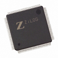
Z8018233ASG Zilog, Z8018233ASG Datasheet - Page 63

Z8018233ASG
Manufacturer Part Number
Z8018233ASG
Description
IC 33MHZ STATIC MIMIC 100-LQFP
Manufacturer
Zilog
Datasheet
1.Z8018233FSG.pdf
(109 pages)
Specifications of Z8018233ASG
Processor Type
Z180
Features
Smart Peripheral Controller
Speed
33MHz
Voltage
5V
Mounting Type
Surface Mount
Package / Case
100-LQFP
Processor Series
Z8018xx
Core
Z80
Data Bus Width
8 bit
Program Memory Type
ROMLess
Interface Type
UART
Maximum Clock Frequency
33 MHz
Number Of Programmable I/os
24
Number Of Timers
2
Operating Supply Voltage
4.5 V to 5.5 V
Maximum Operating Temperature
+ 70 C
Mounting Style
SMD/SMT
Minimum Operating Temperature
0 C
Lead Free Status / RoHS Status
Lead free / RoHS Compliant
Available stocks
Company
Part Number
Manufacturer
Quantity
Price
16550 MIMIC INTERFACE REGISTERS
MIMIC Master Control Register (MMC)
The 16550 MIMIC interface is controlled by the MMC
register. Setting it allows for different modes of operation
such as using the 8-bit counters, DMA accesses, and
which IRQ structure is used with the PC/XT/AT.
Bit 7 Transmit Emulation Delay Counter Enable
(Read/Write)
If bit 7 is set to 1, it enables the transmit delay timer. When
the Z180 reads the Transmit Register, it loads the transmit
delay timer from the Transmit Time Constant Register and
enables the timer to count down to zero. This timer delays
setting the Transmit Holding Register Empty (THRE) bit
until the timer times out. If this bit is 0, then THRE is set
immediately on a Z180 read of the Transmit Register. This
bit also enables the emulation timer used in Transmitter
Double Buffering.
Bit 6 Receive Emulation Delay Counter Enable
(Read/Write)
If bit 6 is set to 1, it enables the receive delay timer. When
the Z180 writes to the Receive Buffer, it loads the receive
delay timer from the Receive Time Constant Register and
enables the timer to count down to zero. This timer delays
setting the Data Ready (DR) bit in the LSR until the timer
times out. If this bit is 0 then DR is set immediately on a Z180
write to the Receive Buffer.
DS971820600
Zilog
D7 D6 D5 D4 D3 D2 D1 D0
0
0
Figure 60. MIMIC Master Control Register
(Z180 MPU Read/Write, Address xxFFH)
0
0
0
0
0
0
VIS Vector Include Status
0 Mode 0 Interrupts
1 Mode 2 Interrupts
HINTR
00 Normal
01 Wire And
10 Out 2 Control
11 Reserved
Rx DMA Enable
Tx DMA Enable
Rx Timer Enable
Tx Timer Enable
Rx DMA
Tx DMA
1=Chan 1 Z180
0=Chan 1 Z180
1=Chan 0 Z180
0=Chan 0 Z180
P R E L I M I N A R Y
PS009801-0301
Both counters are single pass and stop on a count of Zero.
Their purpose is to delay data transfer just as if the 16550
UART had to shift the data in and out. This is provided to
alleviate any software problems a high speed continuous
data transfer might cause to existing software. If this is not
a concern, then data can be read and written as fast as the
two machines can access the devices. In FIFO mode of
operation , the timers are used to delay the status to the PC
interface by the time required to actually shift the characters
out, or in, if an actual UART were present.
Bit 5 Transmit DMA Enable (Read/Write)
If this bit is set to 1, it enables the Transmit DMA function.
Bit 4 Receive DMA Enable (Read/Write)
If this bit is set to 1, it enables the Receive DMA function.
Bit 3 Receive DMA Channel Select (Read/Write)
If bit 3 is set to 0, then Receive DMA transfer is done
through Z180 DMA channel 0 and the Transmit DMA is
done through DMA channel 1. If bit 3 is set to 1, then
Receive DMA transfer is done through Z180 DMA channel
1 and the Transmit DMA is done through DMA channel 0.
Bits 2,1 Interrupt Select (Read/Write).
See Table 15.
Bit 0 Vector Include Status (Read/Write)
This bit is used to select the interrupt response mode of the
Z180. A 0 in this bit enables Mode 0 interrupts; a 1 enables
Mode 2 response.
Bit 2
0
0
1
1
Table 15. MIMIC Master Control Register
Bit 1
0
1
0
1
HINTR Function
HINTR is set to normal 16550 MIMIC mode.
A fully driven output is required when
external priority arbiters are used.
A wired AND condition on the HINTR pin is
possible to the PC/XT/AT. The interrupt
is active High with only the pull-up
of the HINTR pin driving; otherwise this
pin is tri-state. Wired AND is needed when
an external arbiter is not available.
HINTR is driven when out 2 of the Modem
Control Register is 1. HINTR is tri-state
when MCR out 2 is 0.
RESERVED
Interrupt Select
Z
ILOG
I
NTELLIGENT
Z80182/Z8L182
P
ERIPHERAL
3-63


