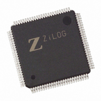
Z8018233ASG Zilog, Z8018233ASG Datasheet - Page 69

Z8018233ASG
Manufacturer Part Number
Z8018233ASG
Description
IC 33MHZ STATIC MIMIC 100-LQFP
Manufacturer
Zilog
Datasheet
1.Z8018233FSG.pdf
(109 pages)
Specifications of Z8018233ASG
Processor Type
Z180
Features
Smart Peripheral Controller
Speed
33MHz
Voltage
5V
Mounting Type
Surface Mount
Package / Case
100-LQFP
Processor Series
Z8018xx
Core
Z80
Data Bus Width
8 bit
Program Memory Type
ROMLess
Interface Type
UART
Maximum Clock Frequency
33 MHz
Number Of Programmable I/os
24
Number Of Timers
2
Operating Supply Voltage
4.5 V to 5.5 V
Maximum Operating Temperature
+ 70 C
Mounting Style
SMD/SMT
Minimum Operating Temperature
0 C
Lead Free Status / RoHS Status
Lead free / RoHS Compliant
Available stocks
Company
Part Number
Manufacturer
Quantity
Price
16550 MIMIC REGISTERS
The Z80182/Z8L182 contains the following set of registers
for interfacing with the PC/XT/AT.
These registers emulate the 16550 UART and enable the
PC/XT/AT to interface with them as with an actual 16550
UART. This allows the Z80182/Z8L182 to be software
compatible with existing modem software.
Receive Buffer Register
When the Z180 has assembled a byte of data to pass to the
PC/XT/AT, it places it in the Receive Buffer Register. If the
Received Data Available interrupt is enabled then an
interrupt is generated for the PC/XT/AT and the Data Ready
bit is set (if the Receive Timer is enabled, the interrupt and
setting of the Data Ready bit is delayed until after the timer
times out). Also the shadowed bits of the Line Status
Register are transferred to their respective bits when the
Z180 MPU writes to the Receive Buffer Register (See Line
Status Register Bits 1, 2, 3 and 4). This allows a simultaneous
setting of error bits when the data is written to the Receive
Buffer Register. In FIFO, mode this address is used to read
(PC) and write (Z180) the Receive FIFO.
DS971820600
Zilog
(PC Read Only, Address 00H, DLAB=0, R/W=Read)
– Receive Buffer Register
– Transmit Holding Register
– Interrupt Enable Register
– Interrupt Identification Register
– FIFO Control Register
– Line Control Register
– Modem Control Register
– Line Status Register
– Modem Status Register
– Scratch Register
– Divisor Latch Least/Most Significant Bytes
– FIFO Control Register
D7 D6 D5 D4 D3 D2 D1 D0
0
(Z180
0
Figure 69. Receive Buffer Register
0
™
MPU Write Only, Address XXF0H)
0
0
0
0
0
Receive Buffer Register
P R E L I M I N A R Y
PS009801-0301
Transmit Holding Register
When the PC/XT/AT writes to the Transmit Holding Register,
the Z80182/Z8L182 responds by setting the appropriate
bit in the IP register and by generating an interrupt to the
Z180 MPU if it is enabled. When the Z180 MPU reads this
register the Transmit Holding Register empty flag is set (if
the transmitter timer is enabled , this bit is set after the timer
times out). In FIFO mode of operation, this address is used
to read (Z180) and write (PC) the Transmitter FIFO.
D7 D6 D5 D4 D3 D2 D1 D0
0
D7 D6 D5 D4 D3 D2 D1 D0
(PC Write Only, Address 00H, DLAB=0, R/W=Write)
0
0
0
(Z180 MPU Read Only, Address xxF0H)
(Z180 MPU Read Only, Address xxE9H)
Figure 70. Transmit Holding Register
0
0
Figure 71. FIFO Control Register
0
(PC Write Only, Address 02H)
0
0
0
0
0
0
0
0
0
FIFO Enable
RCVR FIFO Reset
DMA Mode Select
XMIT FIFO Reset
Reserved (Tx Overrun, MPU only)
Reserved (FCR Write, MPU only)
RCVR Trigger (LSB)
RCVR Trigger (MSB)
Transmitter Holding Register
Z
ILOG
I
NTELLIGENT
Z80182/Z8L182
P
ERIPHERAL
3-69


