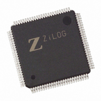
Z8018233ASG Zilog, Z8018233ASG Datasheet - Page 7

Z8018233ASG
Manufacturer Part Number
Z8018233ASG
Description
IC 33MHZ STATIC MIMIC 100-LQFP
Manufacturer
Zilog
Datasheet
1.Z8018233FSG.pdf
(109 pages)
Specifications of Z8018233ASG
Processor Type
Z180
Features
Smart Peripheral Controller
Speed
33MHz
Voltage
5V
Mounting Type
Surface Mount
Package / Case
100-LQFP
Processor Series
Z8018xx
Core
Z80
Data Bus Width
8 bit
Program Memory Type
ROMLess
Interface Type
UART
Maximum Clock Frequency
33 MHz
Number Of Programmable I/os
24
Number Of Timers
2
Operating Supply Voltage
4.5 V to 5.5 V
Maximum Operating Temperature
+ 70 C
Mounting Style
SMD/SMT
Minimum Operating Temperature
0 C
Lead Free Status / RoHS Status
Lead free / RoHS Compliant
Available stocks
Company
Part Number
Manufacturer
Quantity
Price
Z180 MPU DMA SIGNALS
/TEND0. Transfer End 0 (output, active Low). This output
is asserted active during the last write cycle of a DMA
operation. It is used to indicate the end of the block
transfer. /TEND0 is multiplexed with CKA1 on the
CKA1//TEND0 pin.
/TEND1. Transfer End 1 (output, active Low). This output
is asserted active during the last write cycle of a DMA
operation. It is used to indicate the end of the block
transfer. /TEND1 is multiplexed with the ESCC signal
/RTSB and the 16550 MIMIC interface signal /HRxRDY on
the /TEND1//RTSB//HRxRDY pin.
Z180
T
output from PRT channel 1. This line is multiplexed with
A18 of the address bus on the A18/T
Z85230 ESCC
TxDA. Transmit Data (output, active High). This output
signal transmits channel A’s serial data at standard TTL
levels. This output can be tri-stated during power down
modes.
TxDB. Transmit Data (output, active High). This output
signal transmits channel B’s serial data at standard TTL
levels. In Z80182/Z8L182 mode 1, TxDB is multiplexed
with the 16550 MIMIC interface /HDDIS signal on the
TxDB//HDDIS pin.
RxDA. Receive Data (inputs, active High). These inputs
receive channel A’s serial data at standard TTL levels.
RxDB. Receive Data (input, active High). These inputs
receive channel B’s serial data at standard TTL levels. In
Z80182/Z8L182 mode 1 RxDB is multiplexed with the
16550 MIMIC HA1 input on the RxDB/HA1 pin.
/TRxCA. Transmit/Receive Clock (input or output, active
Low). The functions of this pin are under channel A program
control. /TRxCA may supply the receive clock or the
transmit clock in the Input mode or supply the output of the
digital phase-locked loop, the crystal oscillator, the baud
rate generator, or the transmit clock in the output mode.
/TRxCB. Transmit/Receive Clock (input or output, active
Low). The functions of this pin are under channel B program
DS971820600
Zilog
OUT.
Timer Out (output, active High). T
™
MPU TIMER SIGNALS
™
SIGNALS
OUT
pin.
OUT
PS009801-0301
P R E L I M I N A R Y
is the pulse
/DREQ0. DMA request 0 (input, active Low). /DREQ0 is
used to request a DMA transfer from DMA channel 0. The
DMA channel monitors the input to determine when an
external device is ready for a read or write operation. This
input can be programmed to be either level or edge
sensed. /DREQ0 is multiplexed with CKA0 on the
CKA0//DREQ0 pin.
/DREQ1. DMA request 1 (input, active Low). /DREQ1 is
used to request a DMA transfer from DMA channel 1. The
DMA channel monitors the input to determine when an
external device is ready for a read or write operation. This
input can be programmed to be either level or edge
sensed.
control. /TRxCB may supply the receive clock or the
transmit clock in the input mode or supply the output of the
Digital Phase-Locked Loop (DPLL), the crystal oscillator,
the baud rate generator, or the transmit clock in output
mode. In Z80182/Z8L182 mode 1 /TRxCB is multiplexed
with the 16550 MIMIC interface HA0 input on the
/TRxCB/HA0 pin.
/RTxCA. Receive/Transmit Clock (input, active Low). The
functions of this pin are under channel A program control.
In channel A, /RTxCA may supply the receive clock, the
transmit clock, the clock for the baud rate generator, or the
clock for the DPLL. This pin can also be programmed for
use by the /SYNCA pin as a crystal oscillator. The receive
clock may be 1, 16, 32, or 64 times the data rate in
asynchronous mode.
/RTxCB. Receive/Transmit Clock (input, active Low). The
functions of this pin are under channel B program control.
In channel B, /RTxCB may supply the receive clock, the
transmit clock, the clock for the baud rate generator, or the
clock for the DPLL. This pin can also be programmed for
use by the /SYNCB pin as a crystal oscillator. The receive
clock may be 1, 16, 32, or 64 times the data rate in
asynchronous mode. In Z80182/Z8L182 mode 1 the
/RTxCB signal is multiplexed with 16550 MIMIC interface
HA2 input on the /RTxCB/HA2 pin.
Z
ILOG
I
NTELLIGENT
Z80182/Z8L182
P
ERIPHERAL
3-7


