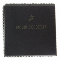
MC68HC000EI16 Freescale Semiconductor, MC68HC000EI16 Datasheet - Page 52

MC68HC000EI16
Manufacturer Part Number
MC68HC000EI16
Description
IC MPU 32BIT 16MHZ 68-PLCC
Manufacturer
Freescale Semiconductor
Specifications of MC68HC000EI16
Processor Type
M680x0 32-Bit
Speed
16MHz
Voltage
3.3V, 5V
Mounting Type
Surface Mount
Package / Case
68-PLCC
Family Name
M68000
Device Core
ColdFire
Device Core Size
16/32Bit
Frequency (max)
16MHz
Instruction Set Architecture
RISC
Supply Voltage 1 (typ)
5V
Operating Supply Voltage (max)
5.25V
Operating Supply Voltage (min)
4.75V
Operating Temp Range
0C to 70C
Operating Temperature Classification
Commercial
Mounting
Surface Mount
Pin Count
68
Package Type
PLCC
Lead Free Status / RoHS Status
Lead free / RoHS Compliant
Features
-
Lead Free Status / Rohs Status
Compliant
Available stocks
Company
Part Number
Manufacturer
Quantity
Price
Company:
Part Number:
MC68HC000EI16
Manufacturer:
TI
Quantity:
604
Company:
Part Number:
MC68HC000EI16
Manufacturer:
FREESCALE
Quantity:
2 900
Company:
Part Number:
MC68HC000EI16
Manufacturer:
Freescale Semiconductor
Quantity:
10 000
Company:
Part Number:
MC68HC000EI16R2
Manufacturer:
FREESCAL
Quantity:
8 831
Company:
Part Number:
MC68HC000EI16R2
Manufacturer:
Freescale Semiconductor
Quantity:
10 000
The descriptions of the eight states of a write cycle are as follows:
STATE 0
STATE 1
STATE 2
STATE 3
STATE 4
STATE 5
STATE 6
5-6
FC2–FC0
*INTERNAL SIGNAL ONLY
D15–D8
A23–A1
DTACK
D7–D0
UDS
CLK
LDS
R/W
A0
AS
*
The write cycle starts in S0. The processor places valid function codes on
FC2–FC0 and drives R/W high (if a preceding write cycle has left R/W low).
During S3, the data bus is driven out of the high-impedance state as the
data to be written is placed on the bus.
At the rising edge of S4, the processor asserts U D S , or LDS. The
processor waits for a cycle termination signal (DTACK or BERR) or VPA, an
M6800 peripheral signal. When VPA is asserted during S4, the cycle
becomes a peripheral cycle (refer to Appendix B M6800 Peripheral
Interface. If neither termination signal is asserted before the falling
edge at the end of S4, the processor inserts wait states (full clock cycles)
until either DTACK or BERR is asserted.
During S5, no bus signals are altered.
During S6, no bus signals are altered.
Entering S1, the processor drives a valid address on the address bus.
On the rising edge of S2, the processor asserts AS and drives R/W low.
Figure 5-7. Word and Byte Write-Cycle Timing Diagram
S0 S1 S2 S3 S4 S5 S6 S7 S0 S1 S2 S3 S4 S5 S6 S7 S0 S1 S2 S3 S4 S5 S6 S7
M68000 8-/16-/32-BIT MICROPROCESSORS USER'S MANUAL
WORD WRITE
Freescale Semiconductor, Inc.
For More Information On This Product,
Go to: www.freescale.com
ODD BYTE WRITE
EVEN BYTE WRITE
MOTOROLA


