MC68HC000EI16 Freescale Semiconductor, MC68HC000EI16 Datasheet - Page 8
MC68HC000EI16
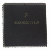
Manufacturer Part Number
MC68HC000EI16
Description
IC MPU 32BIT 16MHZ 68-PLCC
Manufacturer
Freescale Semiconductor
Specifications of MC68HC000EI16
Processor Type
M680x0 32-Bit
Speed
16MHz
Voltage
3.3V, 5V
Mounting Type
Surface Mount
Package / Case
68-PLCC
Family Name
M68000
Device Core
ColdFire
Device Core Size
16/32Bit
Frequency (max)
16MHz
Instruction Set Architecture
RISC
Supply Voltage 1 (typ)
5V
Operating Supply Voltage (max)
5.25V
Operating Supply Voltage (min)
4.75V
Operating Temp Range
0C to 70C
Operating Temperature Classification
Commercial
Mounting
Surface Mount
Pin Count
68
Package Type
PLCC
Lead Free Status / RoHS Status
Lead free / RoHS Compliant
Features
-
Lead Free Status / Rohs Status
Compliant
Available stocks
Company
Part Number
Manufacturer
Quantity
Price
Company:

Part Number:
MC68HC000EI16
Manufacturer:
TI
Quantity:
604
Company:
Part Number:
MC68HC000EI16
Manufacturer:
FREESCALE
Quantity:
2 900
Company:
Part Number:
MC68HC000EI16
Manufacturer:
Freescale Semiconductor
Quantity:
10 000
Company:
Part Number:
MC68HC000EI16R2
Manufacturer:
FREESCAL
Quantity:
8 831
Company:
Part Number:
MC68HC000EI16R2
Manufacturer:
Freescale Semiconductor
Quantity:
10 000


Number
Figure
5-15
5-16
5-17
5-18
5-19
5-20
5-21
5-22
5-23
5-24
5-25
5-26
5-27
5-28
5-29
5-30
5-31
5-32
5-33
5-34
5-35
5-36
5-37
6-1
6-2
6-3
6-4
6-5
6-6
6-7
6-8
6-9
10-1
10-2
10-3
10-4
10-5
10-6
MOTOROLA
3-Wire Bus Arbitration Timing Diagram
(NA to 48-Pin MC68008 and MC68EC000 ........................................................ 5-13
2-Wire Bus Arbitration Timing Diagram.............................................................. 5-14
External Asynchronous Signal Synchronization ................................................. 5-16
Bus Arbitration Unit State Diagrams................................................................... 5-17
3-Wire Bus Arbitration Timing Diagram—Processor Active ............................... 5-18
3-Wire Bus Arbitration Timing Diagram—Bus Active ......................................... 5-19
3-Wire Bus Arbitration Timing Diagram—Special Case ................................ ..... 5-20
2-Wire Bus Arbitration Timing Diagram—Processor Active ............................... 5-21
2-Wire Bus Arbitration Timing Diagram—Bus Active ......................................... 5-22
2-Wire Bus Arbitration Timing Diagram—Special Case ................................ ..... 5-23
Bus Error Timing Diagram .................................................................................. 5-24
Delayed Bus Error Timing Diagram (MC68010)................................................. 5-25
Retry Bus Cycle Timing Diagram ....................................................................... 5-26
Delayed Retry Bus Cycle Timing Diagram ......................................................... 5-27
Halt Operation Timing Diagram.......................................................................... 5-28
Reset Operation Timing Diagram....................................................................... 5-29
Fully Asynchronous Read Cycle ........................................................................ 5-32
Fully Asynchronous Write Cycle......................................................................... 5-33
Pseudo-Asynchronous Read Cycle ................................................................... 5-34
Pseudo-Asynchronous Write Cycle.................................................................... 5-35
Synchronous Read Cycle................................................................................... 5-37
Synchronous Write Cycle ................................................................................... 5-38
Input Synchronizers ........................................................................................... 5-38
Exception Vector Format...................................................................................... 6-4
Peripheral Vector Number Format ....................................................................... 6-5
Address Translated from 8-Bit Vector Number ................................................... 6-5
Exception Vector Address Calculation (MC68010) .............................................. 6-5
Group 1 and 2 Exception Stack Frame .............................................................. 6-10
MC68010 Stack Frame ...................................................................................... 6-10
Supervisor Stack Order for Bus or Address Error Exception ............................. 6-17
Exception Stack Order (Bus and Address Error) ............................................... 6-18
Special Status Word Format .............................................................................. 6-19
MC68000 Power Dissipation (P D ) vs Ambient Temperature (T A ) ..................... 10-3
Drive Levels and Test Points for AC Specifications ........................................... 10-6
Clock Input Timing Diagram ............................................................................... 10-9
Read Cycle Timing Diagram ............................................................................ 10-13
Write Cycle Timing Diagram............................................................................. 10-14
MC68000 to M6800 Peripheral Timing Diagram (Best Case) .......................... 10-16
LIST OF ILLUSTRATIONS (Continued)
Freescale Semiconductor, Inc.
For More Information On This Product,
Go to: www.freescale.com
M68000 USER’S MANUAL
Title
Number
Page
xiii
Related parts for MC68HC000EI16
Image
Part Number
Description
Manufacturer
Datasheet
Request
R

Part Number:
Description:
Manufacturer:
Freescale Semiconductor, Inc
Datasheet:
Part Number:
Description:
Manufacturer:
Freescale Semiconductor, Inc
Datasheet:
Part Number:
Description:
Manufacturer:
Freescale Semiconductor, Inc
Datasheet:
Part Number:
Description:
Manufacturer:
Freescale Semiconductor, Inc
Datasheet:
Part Number:
Description:
Manufacturer:
Freescale Semiconductor, Inc
Datasheet:
Part Number:
Description:
Manufacturer:
Freescale Semiconductor, Inc
Datasheet:
Part Number:
Description:
Manufacturer:
Freescale Semiconductor, Inc
Datasheet:
Part Number:
Description:
Manufacturer:
Freescale Semiconductor, Inc
Datasheet:
Part Number:
Description:
Manufacturer:
Freescale Semiconductor, Inc
Datasheet:
Part Number:
Description:
Manufacturer:
Freescale Semiconductor, Inc
Datasheet:
Part Number:
Description:
Manufacturer:
Freescale Semiconductor, Inc
Datasheet:
Part Number:
Description:
Manufacturer:
Freescale Semiconductor, Inc
Datasheet:
Part Number:
Description:
Manufacturer:
Freescale Semiconductor, Inc
Datasheet:
Part Number:
Description:
Manufacturer:
Freescale Semiconductor, Inc
Datasheet:
Part Number:
Description:
Manufacturer:
Freescale Semiconductor, Inc
Datasheet: