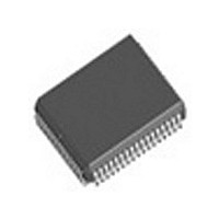
EE80C186XL20 Intel, EE80C186XL20 Datasheet - Page 7

EE80C186XL20
Manufacturer Part Number
EE80C186XL20
Description
IC MPU 16BIT 5V 20MHZ 68PLCC
Manufacturer
Intel
Datasheet
1.S80C188XL25.pdf
(48 pages)
Specifications of EE80C186XL20
Processor Type
80C186
Features
XL suffix, 16-Bit
Speed
20MHz
Voltage
5V
Mounting Type
Surface Mount
Package / Case
68-PLCC
Family Name
Intel186
Device Core
80186
Device Core Size
16b
Frequency (max)
20MHz
Supply Voltage 1 (typ)
5V
Operating Supply Voltage (max)
5.5V
Operating Supply Voltage (min)
4.5V
Operating Temp Range
0C to 70C
Operating Temperature Classification
Commercial
Mounting
Surface Mount
Pin Count
68
Package Type
PLCC
Lead Free Status / RoHS Status
Lead free / RoHS Compliant
Other names
863545
Available stocks
Company
Part Number
Manufacturer
Quantity
Price
Company:
Part Number:
EE80C186XL20
Manufacturer:
INT
Quantity:
2 530
Company:
Part Number:
EE80C186XL20
Manufacturer:
Intel
Quantity:
700
Part Number:
EE80C186XL20
Manufacturer:
INTEL
Quantity:
20 000
DRAM Refresh Control Unit
The Refresh Control Unit (RCU) automatically gen-
erates DRAM refresh bus cycles The RCU operates
only in Enhanced Mode After a programmable peri-
od of time the RCU generates a memory read re-
quest to the BIU If the address generated during a
refresh bus cycle is within the range of a properly
programmed chip select that chip select will be acti-
vated when the BIU executes the refresh bus cycle
Power-Save Control
The 80C186XL when in Enhanced Mode can enter
a power saving state by internally dividing the proc-
essor clock frequency by a programmable factor
This divided frequency is also available at the
CLKOUT pin
All internal logic including the Refresh Control Unit
and the timers have their clocks slowed down by
the division factor To maintain a real time count or a
fixed DRAM refresh rate these peripherals must be
re-programmed when entering and leaving the pow-
er-save mode
Interface for 80C187 Math
Coprocessor (80C186XL Only)
In Enhanced Mode three of the mid-range memory
chip selects are redefined according to Table 1 for
use with the 80C187 The fourth chip select MCS2
functions as in compatible mode and may be pro-
grammed for activity with ready logic and wait states
accordingly As in Compatible Mode MCS2 will func-
tion for one-fourth a programmed block size
ONCE Test Mode
To facilitate testing and inspection of devices when
fixed into a target system the 80C186XL has a test
mode available which allows all pins to be placed in
a high-impedance state ONCE stands for ‘‘ON Cir-
cuit Emulation’’ When placed in this mode the
80C186XL will put all pins in the high-impedance
state until RESET
The ONCE mode is selected by tying the UCS and
the LCS LOW during RESET These pins are sam-
pled on the low-to-high transition of the RES pin
The UCS and the LCS pins have weak internal pull-
up resistors similar to the RD and TEST BUSY pins
to guarantee ONCE Mode is not entered inadver-
tently during normal operation LCS and UCS must
be held low at least one clock after RES goes high
to guarantee entrance into ONCE Mode
Compatible
MCS0
MCS1
MCS2
MCS3
Mode
Table 1 MCS Assignments
PEREQ Processor Extension Request
ERROR NPX Error
MCS2
NPS
Mid-Range Chip Select
Numeric Processor Select
Enhanced Mode
80C186XL 80C188XL
7


