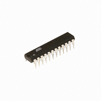
ATF20V8B-10PU Atmel, ATF20V8B-10PU Datasheet

ATF20V8B-10PU
Specifications of ATF20V8B-10PU
Available stocks
Related parts for ATF20V8B-10PU
ATF20V8B-10PU Summary of contents
Page 1
... No Internal Connection VCC +5V Supply I , Active TSSOP CLK/ VCC GND 12 13 OE/IN DIP/SOIC PLCC CLK/ VCC GND 12 13 OE/IN High- performance EE PLD ATF20V8B ATF20V8BQ ATF20V8BQL 25 I/O 24 I I/O 20 I/O Rev. 0407J–07/06 I ...
Page 2
... ATF20V8B(Q)(L) 2 these options significantly reduces total system power and enhances system reliability. The ATF20V8Bs incorporate a superset of the generic architectures, which allows direct replacement of the 20R8 family and most 24-pin combinatorial PLDs. Eight outputs are each allocated eight product terms. Three different modes of operation, configured automatically with soft- ware, allow highly complex logic functions to be realized ...
Page 3
DC Characteristics Symbol Parameter Condition Input or I/O Low 0 ≤ Leakage Current Input or I/O High 3.5 ≤ Leakage Current V Power Supply Current, Standby Outputs Open V Clocked Power ...
Page 4
... PXZ Note: 1. See ordering information for valid part numbers and speed grades. 2. Shaded -25 parts are obsolete with a last-time buy date of August 19, 1999. 3. Shaded -7 and -15 parts are obsolete with a last-time buy date of September 30, 2006. ATF20V8B(Q)( Min Max 8 outputs switching 3 7.5 1 output switching ...
Page 5
... OUT Note: 1. Typical values for nominal supply voltage. This parameter is only sampled and is not 100% tested. Power-up Reset The registers in the ATF20V8Bs are designed to reset dur- ing power-up point delayed slightly from all registers will be reset to the low state result, RST the registered output state will always be high on power-up ...
Page 6
... ATF20V8B architecture. Eight configurable macrocells can be configured as a registered output, combinatorial I/O, combinatorial output, or dedicated input. The ATF20V8B can be configured in one of three different modes. Each mode makes the ATF20V8B look like a dif- ferent device. Most PLD compilers can choose the right mode automatically ...
Page 7
... P20V8 Tango-PLD G20V8 Note: 1. Only applicable for version 3.4 or lower. ATF20V8B Registered Mode PAL Device Emulation/PAL Replacement. The registered mode is used if one or more registers are required. Each macrocell can be configured as either a registered or com- binatorial output or I/ input. For a registered out- put or I/O, the output is enabled by the OE pin, and the register is clocked by the CLK pin ...
Page 8
... Registered Mode Logic Diagram ATF20V8B(Q)(L) 8 ...
Page 9
... In this mode, each macrocell has seven product terms going to the sum term and one product term enabling the output. Complex Mode Operation ATF20V8B Simple Mode PAL Device Emulation/PAL Replacement. In the Simple Mode, 8 product terms are allocated to the sum term. Pins 15 and 16 (center macrocells) are permanently configured as combinatorial outputs ...
Page 10
... Complex Mode Logic Diagram ATF20V8B(Q)(L) 10 ...
Page 11
Simple Mode Logic Diagram 11 ...
Page 12
... ATF20V8B(Q)(L) 12 ...
Page 13
13 ...
Page 14
... ATF20V8B(Q)(L) 14 ...
Page 15
... ATF20V8B-10PC ATF20V8B-10SC ATF20V8B-10XC ATF20V8B-10JI ATF20V8B-10PI ATF20V8B-10SI ATF20V8B-10XI ATF20V8B-15JC ATF20V8B-15PC ATF20V8B-15SC ATF20V8B-15XC ATF20V8B-15JI ATF20V8B-15PI ATF20V8B-15SI ATF20V8B-15XI Ordering Code ATF20V8B-10JU ATF20V8B-10PU Package Type Package Operation Range 28J Commercial 24P3 (0°C to 70°C) 24S 24X 28J Commercial 24P3 (0°C to 70°C) 24S 24X 28J ...
Page 16
... 7 Note: 1. Shaded parts are obsolete with a last-time buy date of September 30, 2006. ATF20V8BQL Green Package Options (Pb/Halide-free/RoHS Compliant) t (ns) t (ns) t (ns Note: 1. Shaded parts are obsolete with a last-time buy date of September 30, 2006. Using “C” Product for Industrial To use commercial product for Industrial temperature ranges, down-grade one speed grade from the “I” to the “C” device (7 ns “ ...
Page 17
Packaging Information 28J – PLCC 1.14(0.045) X 45˚ 0.51(0.020)MAX 45˚ MAX (3X) Notes: 1. This package conforms to JEDEC reference MS-018, Variation AB. 2. Dimensions D1 and E1 do not include mold protrusion. Allowable protrusion is .010"(0.254 mm) ...
Page 18
... Notes: 1. This package conforms to JEDEC reference MS-001, Variation AF. 2. Dimensions D and E1 do not include mold Flash or Protrusion. Mold Flash or Protrusion shall not exceed 0.25 mm (0.010"). 2325 Orchard Parkway San Jose, CA 95131 R ATF20V8B(Q)( PIN TITLE 24P3, 24-lead (0.300"/7.62 mm Wide) Plastic Dual ...
Page 19
SOIC PIN 1 ID PIN 1 E 0º ~ 8º 2325 Orchard Parkway San Jose, CA 95131 TITLE 24S, 24-lead (0.300" body) Plastic Gull Wing Small Outline (SOIC) COMMON ...
Page 20
... TSSOP Dimensions in Millimeter and (Inches)* JEDEC STANDARD MO-153 AD Controlling dimension: millimeters PIN 1 0º ~ 8º 2325 Orchard Parkway San Jose, CA 95131 R ATF20V8B(Q)(L) 20 0.30(0.012) 0.19(0.007) 4.48(0.176) 4.30(0.169) 0.65(0.0256)BSC 7.90(0.311) 7.70(0.303) 0.15(0.006) 0.05(0.002) 0.75(0.030) 0.45(0.018) TITLE 24X, 24-lead (4.4 mm body width) Plastic Thin Shrink Small Outline Package (TSSOP) 6 ...
Page 21
Revision History Revision Level – Release Date J – July 2006 History Ordering Information tables updated to reflect obsolete parts. 21 ...
Page 22
... Disclaimer: The information in this document is provided in connection with Atmel products. No license, express or implied, by estoppel or otherwise, to any intellectual property right is granted by this document or in connection with the sale of Atmel products. EXCEPT AS SET FORTH IN ATMEL’S TERMS AND CONDI- TIONS OF SALE LOCATED ON ATMEL’S WEB SITE, ATMEL ASSUMES NO LIABILITY WHATSOEVER AND DISCLAIMS ANY EXPRESS, IMPLIED OR STATUTORY WARRANTY RELATING TO ITS PRODUCTS INCLUDING, BUT NOT LIMITED TO, THE IMPLIED WARRANTY OF MERCHANTABILITY, FITNESS FOR A PARTICULAR PURPOSE, OR NON-INFRINGEMENT ...


