UDA1345TS/N2,112 NXP Semiconductors, UDA1345TS/N2,112 Datasheet
UDA1345TS/N2,112
Specifications of UDA1345TS/N2,112
935266777112
UDA1345TSDB
Available stocks


Related parts for UDA1345TS/N2,112


UDA1345TS/N2,112 Summary of contents
Page 1
DATA SHEET UDA1345TS Economy audio CODEC Product specification Supersedes data of 2000 Dec 19 INTEGRATED CIRCUITS 2002 May 28 ...
Page 2
... NXP Semiconductors Economy audio CODEC CONTENTS 1 FEATURES 1.1 General 1.2 Multiple format input interface 1.3 DAC digital sound processing 1.4 Advanced audio configuration 2 GENERAL DESCRIPTION 3 ORDERING INFORMATION 4 QUICK REFERENCE DATA 5 BLOCK DIAGRAM 6 PINNING 7 FUNCTIONAL DESCRIPTION 7.1 Analog-to-Digital Converter (ADC) 7.2 Analog front-end 7 ...
Page 3
... NXP Semiconductors Economy audio CODEC 1 FEATURES 1.1 General • Low power consumption • 2.4 to 3.6 V power supply range with 3.0 V typical • tolerant TTL compatible digital inputs • 256, 384 and 512f system clock s • Supports sampling frequencies from 8 to 100 kHz • ...
Page 4
... NXP Semiconductors Economy audio CODEC 4 QUICK REFERENCE DATA SYMBOL PARAMETER Supplies V ADC analog supply voltage DDA(ADC) V DAC analog supply voltage DDA(DAC) V digital supply voltage DDD I ADC analog supply current DDA(ADC) I DAC analog supply current DDA(DAC) I DAC operational amplifier supply current DDO(DAC) ...
Page 5
... NXP Semiconductors Economy audio CODEC SYMBOL PARAMETER Power performance P power consumption in record and playback ADDA mode P power consumption in playback only mode DA P power consumption in record only mode AD P power consumption in Power-down mode PD Notes 1. The input voltage can (RMS) when the current through the ADC input pin is limited to approximately using a series resistor ...
Page 6
... NXP Semiconductors Economy audio CODEC 5 BLOCK DIAGRAM V DDA(ADC) V SSA(ADC) handbook, full pagewidth 3 VINL 10 V DDD 11 V SSD 18 DATAO 16 BCK DATAI 9 MP1 UDA1345TS 26 VOUTL 2002 May 28 V ADCP dB/6 dB SWITCH ADC ADC DECIMATION FILTER DC-CANCELLATION FILTER DIGITAL INTERFACE INTERPOLATION FILTER NOISE SHAPER ...
Page 7
... NXP Semiconductors Economy audio CODEC 6 PINNING SYMBOL PIN V 1 analog ground pad SSA(ADC analog supply pad DDA(ADC) VINL 3 analog input pad V 4 analog pad ref(A) VINR 5 analog input pad V 6 analog pad ADCN V 7 analog pad ADCP MC1 tolerant digital input pad with internal pull-down pad ...
Page 8
... NXP Semiconductors Economy audio CODEC handbook, halfpage V SSA(ADC DDA(ADC) 2 VINL 3 V ref(A) 4 VINR 5 V ADCN 6 V ADCP 7 UDA1345TS MC1 8 MP1 9 V DDD 10 V SSD 11 SYSCLK 12 MP2 13 MP3 14 MGS876 Fig.2 Pin configuration. 7 FUNCTIONAL DESCRIPTION The UDA1345TS accommodates slave mode only, this means that in all applications the system devices must provide the system clocks (being the system clock itself and the digital audio interface signals) ...
Page 9
... NXP Semiconductors Economy audio CODEC Table 2 Digital decimation filter characteristics ITEM CONDITIONS 0 − 0.45f Pass-band ripple Stop band >0.55f 0 − 0.45f Dynamic range Overall gain when signal is input to ADC to digital output Note: the digital output level is inversely proportional to the ADC analog power supply. This means that with a constant analog input level and increasing power supply the digital output level will decrease proportionally ...
Page 10
... NXP Semiconductors Economy audio CODEC 7.10 L3 microcontroller mode The UDA1345TS is set to the L3 microcontroller mode by setting both MC1 (pin 8) and MC2 (pin 21) LOW. The definition of the control registers is given in Section 7.12. 7.10.1 P INNING DEFINITION The pinning definition under L3 microcontroller interface is given in Table 5. ...
Page 11
... NXP Semiconductors Economy audio CODEC 7.11.2 S YSTEM CLOCK Under static pin control the options are 256f With pin MP3 (pin 14) the mode can be set as is given in Table 8. Table 8 System clock settings under static pin mode MODE 256f system clock s 384f system clock s 7 ...
Page 12
WS LEFT >= BCK DATA MSB B2 LSB WS LEFT >= BCK DATA MSB B2 LSB MSB WS LEFT 16 BCK DATA MSB WS LEFT BCK DATA MSB B2 ...
Page 13
... NXP Semiconductors Economy audio CODEC 7.12 L3 interface The UDA1345TS has a microcontroller input mode. In the microcontroller mode, all of the digital sound processing features and the system controlling features can be controlled by the microcontroller. The controllable features are: • System clock frequency • Data input format • ...
Page 14
... NXP Semiconductors Economy audio CODEC handbook, full pagewidth L3MODE t h(MA) L3CLOCK L3DATA t halt handbook, full pagewidth L3MODE t s(MT) L3CLOCK L3DATA write 2002 May s(MA) t s(DAT) t h(DAT) BIT 0 Fig.4 Timing address mode h(DAT) BIT 0 Fig.5 Timing for data transfer mode. 14 Product specification ...
Page 15
... NXP Semiconductors Economy audio CODEC handbook, full pagewidth L3MODE L3CLOCK L3DATA Table 13 Data transfer of type status LAST IN TIME BIT 7 BIT 6 BIT 5 BIT SC1 SC0 Table 14 Data transfer of type data LAST IN TIME BIT 7 BIT 6 BIT 5 BIT VC5 VC4 DE1 2002 May 28 t halt ...
Page 16
... NXP Semiconductors Economy audio CODEC 7.12.2.2 System clock frequency A 2-bit value (SC1 and SC0) to select the used external clock frequency (see Table 15). Table 15 System clock frequency settings SC1 SC0 7.12.2.3 Data input format A 3-bit value (IF2 to IF0) to select the used data format (see Table 16) ...
Page 17
... NXP Semiconductors Economy audio CODEC 7.12.2.8 Power control A 2-bit value to disable the ADC and/or DAC to reduce power consumption. Table 21 Power control settings PC1 LIMITING VALUES In accordance with the Absolute Maximum Rating System (IEC 60134). All voltages referenced to ground DDD DDA DDO ...
Page 18
... NXP Semiconductors Economy audio CODEC 10 DC CHARACTERISTICS 3 DDD DDA DDO s (pins 1, 11, 22 and 27); unless otherwise specified. SYMBOL PARAMETER Supplies V ADC analog supply voltage DDA(ADC) V DAC analog supply voltage DDA(DAC) V digital supply voltage DDD I ADC analog supply current DDA(ADC) I DAC analog supply current ...
Page 19
... NXP Semiconductors Economy audio CODEC SYMBOL PARAMETER C input capacitance i Digital-to-analog converter V reference voltage ref( reference output resistance o(ref) ref(D) R DAC output resistance o I maximum output current o(max) R load resistance L C load capacitance L Notes 1. All power supply pins (V and When higher capacitive loads must be driven then a 100 Ω resistor must be connected in series with the DAC output in order to prevent oscillations in the output operational amplifier ...
Page 20
... NXP Semiconductors Economy audio CODEC 11 AC CHARACTERISTICS (ANALOG 3 kHz; f DDD DDA DDO i (pins 1, 11, 22 and 27); unless otherwise specified. SYMBOL PARAMETER Analog-to-digital converter D digital output level (RMS) o input voltage ΔV unbalance between channels i (THD + N)/S total harmonic distortion-plus-noise to signal ratio S/N signal-to-noise ratio α ...
Page 21
... NXP Semiconductors Economy audio CODEC 12 AC CHARACTERISTICS (DIGITAL 2 DDD DDA DDO (pins 1, 11, 22 and 27); unless otherwise specified. SYMBOL PARAMETER System clock timing; see Fig.7 T system clock cycle sys t f LOW-level pulse width CWL sys t f HIGH-level pulse width CWH ...
Page 22
... NXP Semiconductors Economy audio CODEC SYMBOL PARAMETER t L3DATA set-up time s(DAT) t L3DATA hold time h(DAT) t L3MODE halt time halt Notes 1. Sampling range from 5 to 100 kHz is supported, with f 2. Sampling range from kHz is supported, with f t CWH handbook, full pagewidth handbook, full pagewidth ...
Page 23
... NXP Semiconductors Economy audio CODEC 13 APPLICATION INFORMATION The application information as given in Fig optimum application environment. Simplification is possible at the cost of some performance degradation. The following notes apply: • The capacitors at the output of the DAC can be reduced. It should be noted that the cut-off frequency of the DC filter also changes. • ...
Page 24
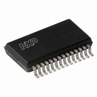
... NXP Semiconductors Economy audio CODEC 14 PACKAGE OUTLINE SSOP28: plastic shrink small outline package; 28 leads; body width 5 pin 1 index 1 e DIMENSIONS (mm are the original dimensions) A UNIT max. 0.21 1. 0.25 0.05 1.65 Note 1. Plastic or metal protrusions of 0.2 mm maximum per side are not included. ...
Page 25
... NXP Semiconductors Economy audio CODEC 15 SOLDERING 15.1 Introduction to soldering surface mount packages This text gives a very brief insight to a complex technology. A more in-depth account of soldering ICs can be found in our “Data Handbook IC26; Integrated Circuit Packages” (document order number 9398 652 90011). ...
Page 26
... NXP Semiconductors Economy audio CODEC 15.5 Suitability of surface mount IC packages for wave and reflow soldering methods PACKAGE BGA, LFBGA, SQFP, TFBGA HBCC, HLQFP, HSQFP, HSOP, HTQFP, HTSSOP, SMS (3) PLCC , SO, SOJ LQFP, QFP, TQFP SSOP, TSSOP, VSO Notes 1. All surface mount (SMD) packages are moisture sensitive. Depending upon the moisture content, the maximum temperature (with respect to time) and body size of the package, there is a risk that internal or external package cracks may occur due to vaporization of the moisture in them (the so called popcorn effect) ...
Page 27
... In no event shall NXP Semiconductors be liable for any indirect, incidental, punitive, special or consequential damages (including - without limitation - lost profits, lost savings, business interruption, costs related to the ...
Page 28
... NXP Semiconductors’ specifications such use shall be solely at customer’s own risk, and (c) customer fully indemnifies NXP Semiconductors for any liability, damages or failed product claims resulting from customer design and use of the product for automotive applications beyond NXP Semiconductors’ ...
Page 29
... Interface, Security and Digital Processing expertise Customer notification This data sheet was changed to reflect the new company name NXP Semiconductors, including new legal definitions and disclaimers. No changes were made to the technical content, except for package outline drawings which were updated to the latest version. ...