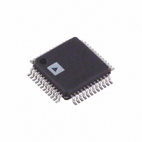
AD1938YSTZ Analog Devices Inc, AD1938YSTZ Datasheet - Page 7

AD1938YSTZ
Manufacturer Part Number
AD1938YSTZ
Description
IC CODEC 24BIT 4ADC/8DAC 48LQFP
Manufacturer
Analog Devices Inc
Type
General Purposer
Datasheet
1.AD1938YSTZRL.pdf
(32 pages)
Specifications of AD1938YSTZ
Data Interface
Serial
Resolution (bits)
24 b
Number Of Adcs / Dacs
4 / 8
Sigma Delta
Yes
S/n Ratio, Adcs / Dacs (db) Typ
94 / 94
Dynamic Range, Adcs / Dacs (db) Typ
105 / 106
Voltage - Supply, Analog
3 V ~ 3.6 V
Voltage - Supply, Digital
3 V ~ 3.6 V
Operating Temperature
-40°C ~ 105°C
Mounting Type
Surface Mount
Package / Case
48-LQFP
Audio Codec Type
Audio
No. Of Adcs
4
No. Of Dacs
8
No. Of Input Channels
4
No. Of Output Channels
8
Adc / Dac Resolution
24bit
Adcs / Dacs Signal To Noise Ratio
108dB
Lead Free Status / RoHS Status
Lead free / RoHS Compliant
Available stocks
Company
Part Number
Manufacturer
Quantity
Price
Company:
Part Number:
AD1938YSTZ
Manufacturer:
NXP
Quantity:
35
Company:
Part Number:
AD1938YSTZ
Manufacturer:
ADI
Quantity:
227
Company:
Part Number:
AD1938YSTZ
Manufacturer:
Analog Devices Inc
Quantity:
10 000
Part Number:
AD1938YSTZ
Manufacturer:
ADI/亚德诺
Quantity:
20 000
Company:
Part Number:
AD1938YSTZRL
Manufacturer:
Analog Devices Inc
Quantity:
10 000
TIMING SPECIFICATIONS
−40°C < T
Table 7.
Parameter
INPUT MASTER CLOCK (MCLK) AND RESET
PLL
SPI PORT
DAC SERIAL PORT
ADC SERIAL PORT
AUXILIARY INTERFACE
t
t
f
f
t
t
Lock time
256 f
t
t
f
t
t
t
t
t
t
t
t
t
t
t
t
t
t
t
t
t
t
t
t
t
t
t
t
t
t
t
t
t
MCLK
MCLK
CCLK
MH
MH
PDR
PDRR
CCH
CCL
CDS
CDH
CLS
CLH
CLH
COE
COD
COH
COTS
DBH
DBL
DLS
DLH
DLS
DDS
DDH
ABH
ABL
ALS
ALH
ALS
ABDD
AXDS
AXDH
DXDD
XBH
XBL
DLS
DLH
MCLKO/XO Pin
S
VCO Clock, Output Duty Cycle,
C
< +125°C, DVDD = 3.3 V ± 10%.
Condition
MCLK duty cycle
MCLK frequency
RST low
RST recovery
MCLK and LR clock input
CCLK high
CCLK low
CCLK frequency
CIN setup
CIN hold
CLATCH setup
CLATCH hold
CLATCH high
COUT enable
COUT delay
COUT hold
COUT tristate
DBCLK high
DBCLK low
DLRCLK setup
DLRCLK hold
DLRCLK skew
DSDATA setup
DSDATA hold
ABCLK high
ABCLK low
ALRCLK setup
ALRCLK hold
ALRCLK skew
ASDATA delay
AAUXDATA setup
AAUXDATA hold
DAUXDATA delay
AUXBCLK high
AUXBCLK low
AUXLRCLK setup
AUXLRCLK hold
Rev. C | Page 7 of 32
Comments
DAC/ADC clock source = PLL clock @ 256 f
384 f
DAC/ADC clock source = direct MCLK @ 512 f
(bypass on-chip PLL)
PLL mode, 256 f
Direct 512 f
Reset to active output
See Figure 11
f
To CCLK rising
From CCLK rising
To CCLK rising
From CCLK falling
Not shown in Figure 11
From CCLK falling
From CCLK falling
From CCLK falling, not shown in Figure 11
From CCLK falling
See Figure 24
Slave mode
Slave mode
To DBCLK rising, slave mode
From DBCLK rising, slave mode
From DBCLK falling, master mode
To DBCLK rising
From DBCLK rising
See Figure 25
Slave mode
Slave mode
To ABCLK rising, slave mode
From ABCLK rising, slave mode
From ABCLK falling, master mode
From ABCLK falling
To AUXBCLK rising
From AUXBCLK rising
From AUXBCLK falling
To AUXBCLK rising
From AUXBCLK rising
CCLK
= 1/t
S
, 512 f
CCP
S
S
, only t
, and 768 f
mode
S
reference
CCP
shown in Figure 11
S
S
,
S
Min
40
40
6.9
15
4096
40
35
35
10
10
10
10
10
30
10
10
10
5
−8
10
5
10
10
10
5
−8
10
5
10
10
10
5
AD1938
Max
60
60
13.8
27.6
10
60
10
30
30
30
+8
+8
18
18
Unit
%
%
MHz
MHz
ns
t
ms
%
ns
ns
MHz
ns
ns
ns
ns
ns
ns
ns
ns
ns
ns
ns
ns
ns
ns
ns
ns
ns
ns
ns
ns
ns
ns
ns
ns
ns
ns
ns
ns
ns
MCLK


