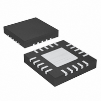
MAX9860ETG+T Maxim Integrated Products, MAX9860ETG+T Datasheet - Page 32

MAX9860ETG+T
Manufacturer Part Number
MAX9860ETG+T
Description
IC CODEC MONO AUD 16BIT 24TQFN
Manufacturer
Maxim Integrated Products
Type
Audio Codecr
Datasheet
1.MAX9860ETG.pdf
(40 pages)
Specifications of MAX9860ETG+T
Data Interface
Serial
Resolution (bits)
16 b
Number Of Adcs / Dacs
1 / 2
Sigma Delta
Yes
Dynamic Range, Adcs / Dacs (db) Typ
81 / 90
Voltage - Supply, Analog
1.7 V ~ 1.9 V
Voltage - Supply, Digital
1.7 V ~ 1.9 V
Operating Temperature
-40°C ~ 85°C
Package / Case
24-TQFN Exposed Pad
Lead Free Status / RoHS Status
Lead free / RoHS Compliant
16-Bit Mono Audio Voice Codec
The MAX9860 includes complete power management
control to minimize power usage. The DAC and both
The MAX9860 includes a revision code to allow easy
identification of the device revision. The current revision
code is 0x40.
The MAX9860 features an I
2-wire serial interface consisting of a serial-data line
(SDA) and a serial-clock line (SCL). SDA and SCL facili-
tate communication between the MAX9860 and the
master at clock rates up to 400kHz. Figure 6 shows the
2-wire interface timing diagram. The master generates
SCL and initiates data transfer on the bus. The master
device writes data to the MAX9860 by transmitting the
proper slave address followed by the register address
and then the data word. Each transmit sequence is
framed by a START (S) or REPEATED START (Sr) con-
dition and a STOP (P) condition. Each word transmitted
to the MAX9860 is 8 bits long and is followed by an
acknowledge clock pulse. A master reading data from
the MAX9860 transmits the proper slave address fol-
lowed by a series of nine SCL pulses. The MAX9860
Table 11. Power Management Register
Table 12. Revision Code Register
SMBus is a trademark of Intel Corp.
32
REGISTER ADDRESS
ADDR
ADCLEN/ADCREN
0xFF
______________________________________________________________________________________
DACEN
SHDN
BITS
0x10
B7
Active-Low Software Shutdown
0 = MAX9860 is in full shutdown.
1 = MAX9860 is powered on.
When SHDN = 0. All register settings are preserved and the I
DAC Enable
0 = DAC disabled.
1 = DAC enabled.
ADC Left/Right Enable
0 = Left/right ADC disabled.
1 = Left/right ADC enabled.
The left ADC must be enabled when using the right ADC.
SHDN
B7
2
Power Management
C/SMBus™-compatible,
I
B6
2
C Serial Interface
Revision Code
B6
0
B5
B5
0
B4
ADCs can be independently enabled so that only the
required circuitry is active.
transmits data on SDA in sync with the master-generat-
ed SCL pulses. The master acknowledges receipt of
each byte of data. Each read sequence is framed by a
START or REPEATED START condition, a not acknowl-
edge, and a STOP condition. SDA operates as both an
input and an open-drain output. A pullup resistor, typi-
cally greater than 500Ω, is required on SDA. SCL oper-
ates only as an input. A pullup resistor, typically greater
than 500Ω, is required on SCL if there are multiple mas-
ters on the bus, or if the single master has an open-
drain SCL output. Series resistors in line with SDA and
SCL are optional. Series resistors protect the digital
inputs of the MAX9860 from high voltage spikes on the
bus lines, and minimize crosstalk and undershoot of the
bus signals.
REV
B4
0
FUNCTION
B3
DACEN
B3
2
C interface remains active.
B2
B2
0
ADCLEN
B1
B1
ADCREN
B0
B0


