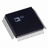
AD1843JS Analog Devices Inc, AD1843JS Datasheet
AD1843JS
Specifications of AD1843JS
Available stocks


Related parts for AD1843JS


AD1843JS Summary of contents
Page 1
FEATURES Single Chip Integrated Speech, Audio, Fax and Modem Codec Highly Configurable Stereo Supports V.34, V.32bis, and Fallback Modem Standards As Well As Voice Over Data Dual Digital Resamplers with Programmable Input and Output Phase and Frequency Three On-Chip ...
Page 2
AD1843–SPECIFICATIONS STANDARD TEST CONDITIONS UNLESS OTHERWISE NOTED Temperature 25 Digital Supply (V ) 5.0 DD Analog Supply (V ) 5.0 CC Sample Rate ( Input Signal 1008 Analog Output Passband kHz ADC FFT ...
Page 3
DIGITAL DECIMATION AND INTERPOLATION FILTERS–AUDIO MODE* Passband Passband Ripple Transition Band 1 Stopband Stopband Rejection Group Delay Group Delay Variation Over Passband DIGITAL DECIMATION AND INTERPOLATION FILTERS–MODEM MODE* Passband Passband Ripple Transition Band 2 Stopband Stopband Rejection Group Delay Group ...
Page 4
AD1843 DAC1 DIGITAL-TO-ANALOG CONVERTERS Audio Dynamic Range (–60 dB Input, THD+N Referenced to Full Scale, A-Weighted, DA1FLT = 0) Audio THD+N (Referenced to Full Scale, DA1FLT = 0) Audio Signal-to-Intermodulation Distortion* (CCIF Method) Interchannel Gain Mismatch (Difference of Gain Errors) ...
Page 5
ANALOG OUTPUT LOUT1 Full-Scale Output Voltage (RMS Values Assume Sine Wave Input) LOUT2 Full-Scale Single-Ended Output Voltage (RMS Values Assume Sine Wave Input) LOUT2 Full-Scale Differential Output Voltage (RMS Values Assume Sine Wave Input) LOUT1 Output Impedance* LOUT2 Output Impedance* ...
Page 6
... Exposure to absolute maximum rating conditions for extended periods may affect device reliability. 6.0 V 6 Model +70 C AD1843JS +150 C AD1843JST V –6– Min Typ Max 4.75 5.25 2.85 5.25 210 250 150 175 60 75 150 175 90 100 1 0.5 ...
Page 7
SDO 1 SDFS 2 GNDD TSI TSO 6 GNDD AUX3R 11 AUX3L 12 AUX2R 13 AUX2L 14 AUX1R 15 AUX1L 16 MICR 17 MICL 18 ...
Page 8
AD1843 100 SDO SDFS GNDD TSI 6 TSO GNDD AUX3R 15 AUX3L 16 AUX2R ...
Page 9
Analog Signals Pin Name PQFP TQFP LINLP 28 35 LINLN 29 36 LINRP 26 33 LINRN 27 34 MICL 18 21 MICR 17 22 AUX1L 16 20 AUX1R 15 19 AUX2L 14 18 AUX2R 13 17 AUX3L 12 16 AUX3R ...
Page 10
AD1843 Miscellaneous Pin Name PQFP TQFP XTALI 61 76 XTALO 62 77 PWRDWN 51 64 RESET 52 65 PDMNFT 49 61 CMOUT REF FILTL 25 31 FILTR 23 29 AAFILTL 24 30 AAFILTR 22 28 ...
Page 11
POWER SUPPLIES Pin Name PQFP TQFP V 20, 41, 44 25, 51 GNDA 21, 37, 40, 48 27, 46, 49 50, 53, 5, 10, 62, 66 63, 64, 68, 72, 79, ...
Page 12
AD1843 µ/A µ/A LAW LAW FIFO ATTN MUTE DAC GN/AT MUTE Figure 2. Detailed Functional Block Diagram –12– µ/A LAW FIFO ATTN MUTE DAC GN/AT MUTE REV. 0 ...
Page 13
On-chip bit and baud clock generation circuitry allows either synchronous or asynchronous operation of the transmit (DAC) and receive (ADC) paths. Each path features independent phase advance and retard adjustments via software control. The AD1843 can also synchronize modem operation ...
Page 14
AD1843 filtered in the analog domain by a combination of switched-capaci- tor and continuous-time filters. They remove the very high fre- quency components of the DAC bitstream output. No external components are required. Phase linearity at the analog output is ...
Page 15
The lock range of these digital PLLs is 4 kHz to 54 kHz, which is the same range supported by the register- controlled clock generators SYNC input ...
Page 16
AD1843 dependent; depending upon the sequence in which the hardware resources are powered down, the savings may be more or less than the typical numbers given. Mode Changing In general, there are very few restrictions with respect to chang- ing ...
Page 17
EXTERNAL WAVEFORM SYNTHESIZER AUDIO FROM AUDIO FROM CD-ROM EXTERNAL MPEG DECODER DAA PSTN PC SPEAKER AUDIO FROM DAT OR CASSETTE SAMPLE PERIOD N SLOT SDI OR SDO MSB SCLK SDFS SAMPLE ...
Page 18
AD1843 SAMPLE PERIOD N SLOT 0 GAP SDI OR SDO MSB SCLK TSI SAMPLE PERIOD N SLOT 0 SDI OR SDO MSB SCLK TSI SAMPLE PERIOD N SLOT ...
Page 19
Modem Data Access Arrangement (DAA) devices are generally differential on the transmit side, and single-ended on the receive side. The DAA transmit input (generally differential) should be connected to the DAC2 output, pins LOUT2LP and LOUT2LN, or LOUT2RP and LOUT2RN. ...
Page 20
AD1843 produced by an AD1843 serving as bus master, an AD1843 serving as bus slave does not actually require these frame sizes. When FRS is set to “1,” a slave will operate correctly with any number or fraction of slots, ...
Page 21
DAC Not Full status bits. Therefore driver software does not have to make provision for frame-to- frame delays between control and status information; the infor- mation in each frame is always up to date. The AD1843 ...
Page 22
AD1843 SERIAL INTERFACE INPUT Note that the references to slot numbers are valid only when the AD1843 is configured in master mode. For slave mode, bus owner- ship does not necessarily start on Slot 0. Control Word Input (Slot 0 ...
Page 23
DAC1 Right Sample Input (Slot 3 or 19) Data 15 Data 14 DATA15 DATA14 Data 7 Data 6 DATA7 DATA6 Data format may be 8-bit unsigned linear PCM, 16-bit signed linear PCM, 8-bit -Law companded, or 8-bit A-Law companded. MSB ...
Page 24
AD1843 SERIAL INTERFACE OUTPUT Status Word Output (Slot 0 or 16) Data 15 Data 14 res res Data 7 Data 6 res res ADRV Right ADC Channel Output Valid Flag. Set to “1” if slot 3 (or 19) contains valid ...
Page 25
Reserved Output (Slots 4 or 20) Data 15 Data 14 res res Data 7 Data 6 res res res Reserved for future expansion. Read back as “0.” Should be ignored to ensure future compatibility. Reserved Output (Slots 5 or 21) ...
Page 26
AD1843 LINLP LINLN LINRP LINRN MICL MICR AUX1L AUX1R AUX2L AUX2R AUX3L AUX3R MIN MUTE MOUT CRA8 MUTE LOUT1L LOUT1R DRIVER CRA8 MUTE HPOUTL HPOUTC HPOUTR LOUT2LP LOUT2LN LOUT2RP LOUT2RN SUML SUMR Figure 12. AD1843 Control Registers Associated with Block ...
Page 27
XTALI CRAX = CONTROL REGISTER ADDRESS “X” CRA25 CRA25 MUTE CRA25 MUTE Figure 13. AD1843 Control Registers Associated with Block Diagram Address Register Description ...
Page 28
AD1843 Address 0 Data 15 Data 14 INIT PDNO Data 7 Data 6 res res This register is read only. INIT Clock Initialization Flag. This bit is set to “1” if the AD1843’s internal clocks generated from the crystal input ...
Page 29
OVL1:0 ADC Left Overrange Detect. These bits record the largest output magnitude on the ADC left channel and are cleared to “00” after any write to this register. The peak amplitude as recorded by these bits is “sticky,” i.e., the ...
Page 30
AD1843 Address 3 Data 15 Data 14 LD2MM res Data 7 Data 6 RD2MM res LD2MM Left DAC2 Mix Mute 0 = Mix Enabled 1 = Mix Muted LD2M4:0 Left DAC2 Mix Gain/Attenuation Select. Least significant bit represents –1.5 dB. ...
Page 31
Reserved for future expansion. To ensure future compatibility, write “0” to all reserved bits. Initial default state after reset: 1000 1000 1000 1000 (8888 hex). Cleared to default and cannot be written to when: the RESET pin is asserted ...
Page 32
AD1843 RX3MM Right Auxiliary 3 Mix Mute 0 = Mix Enabled 1 = Mix Muted RX3M4:0 Right Auxiliary 3 Mix Gain/Attenuation Select. Least significant bit represents –1.5 dB. Referred to 2.0 V p-p DAC1 output level. 00000 = +12.0 dB ...
Page 33
MNM4:0 Left and Right Mono Mix Gain/Attenuation Select. Least significant bit represents –1.5 dB. 00000 = +12.0 dB Gain 01000 = 0.0 dB 11111 = –34.5 dB Attenuation ALLMM All Mix Mute. Mutes all mixing (MIC, AUX1, AUX2, AUX3, and ...
Page 34
AD1843 LDA1G5:0 Left DAC1 Analog/Digital Gain/Attenuation Select. Least significant bit represents –1.5 dB. Note that the implementation of the attenuation is mixed analog and digital. 0 00000 = +12.0 dB: 0 01000 = 0.0 dB: 0 11111 = –34.5 dB: ...
Page 35
Address 11 Output Control—DAC1 Digital Attenuation Data 15 Data 14 LDA1AM res Data 7 Data 6 RDA1AM res LDA1AM Left DAC1 Digital Mute 0 = Left DAC1 Enabled 1 = Left DAC1 Muted LDA1A5:0 Left DAC1 Digital Attenuation Select. Least ...
Page 36
AD1843 Address 13 Digital Mix Control—ADC to DAC1 Data 15 Data 14 LAD1MM res LAD1M5 Data 7 Data 6 RAD1MM res RAD1M5 Restrictions: ADC and DAC channel mixed must receive conversion rate from same Clock Generator. Serial interface must be ...
Page 37
Address 15 Codec Configuration—Channel Sample Rate Source Select Data 15 Data 14 res res Data 7 Data 6 res res DA2C1:0 DAC2 Sample Rate Source. Selects the sample rate clock source for left and right channels of DAC2 ...
Page 38
AD1843 C1VID Clock Generator 1 Video Lock Mode. This bit is used to select between lock modes when the Clock Generator 1 is referenced to SYNC1 (C1REF set to “1”). This bit should be reset to “0” if C1REF is ...
Page 39
NTSC (C1M7 = “0”): Divisor (C1M3:0) 1 (0000) 2 (0001) 3 (0010) 4 (0011) 5 (0100) 6 (0101) 7 (0110) 8 (0111) *When C1M6:4 = “100,” base frequency is 48,000 Hz only if NTSC sync rate is increased by 1001/1000, ...
Page 40
AD1843 overwritten even if all previously programmed phase advance/retard has not been processed. When written, the con- tents of this register (just prior to the write) are transmitted during slot 1 of the following frame (as with all Control Register ...
Page 41
Conversion clock rate established using Control Register Address 20 and the C2X8/7 bit. If the actual Conversion clock differs from the value selected by C2M7:4, then the resultant Bit clock will be different from ...
Page 42
AD1843 Address 20 Clock Generator 2 Control—Sample Rate Data 15 Data 14 C2C15 C2C14 Data 7 Data 6 C2C7 C2C6 C2C15:0 Clock Generator 2 Conversion (Sample) Rate Select. Defines the conversion rate produced by Clock Generator 2 when not referenced ...
Page 43
Clocks are referenced to the input on pin SYNC3 (Sync 3 Clock Input). Sample clock frequency is defined by C3VID and C3M7:0. Sample clock phase is locked to SYNC3 and cannot be shifted. Bit clock frequency is defined ...
Page 44
AD1843 When in Video Lock Mode (C3REF and C3VID are both set to “1”): Bits C3M7:0 select the Conversion clock rate. The most significant bit (C3M7) must be set to indicate the type of video lock, either NTSC or PAL. ...
Page 45
Address 24 Clock Generator 3 Control—Sample Phase Shift Data 15 Data 14 res res Data 7 Data 6 C3P7 C3P6 C3PD Clock Generator 3 Phase Shift Direction. This bit controls the direction of sample clock phase shift Phase ...
Page 46
AD1843 DA1FLT DAC1 (Left and Right Channels) Digital Filter Select. This bit is overridden when DRSFLT is set to “1.” See be- low for filter specifications. This bit can be altered only if DAC1 is powered down. Unlike DA2FLT, this ...
Page 47
DA2SM DAC2 Stereo/Mono Mode Select. When in stereo mode, data transmitted to the AD1843 during slot 4 is used by DAC2 left and data transmitted to the AD1843 during slot 5 is used by DAC2 right. When in mono mode, ...
Page 48
AD1843 Address 27 Codec Configuration—Channel Power Down Data 15 Data 14 DFREE res Data 7 Data 6 ANAEN HPEN DFREE Digital Resource Free. When set to “1,” this bit reduces the level of power down normally achieved by asserting the ...
Page 49
ADREN ADC Right Channel Enable/Power Down. When this bit is reset to “0,” the right ADC channel is powered down and serial interface sample output will cease after the current frame. When this bit is set to “1,” the right ...
Page 50
AD1843 C2EN Clock Generator 2 Enable/Power Down Clock Generator 2 Powered Down 1 = Clock Generator 2 Enabled C1EN Clock Generator 1 Enable/Power Down Clock Generator 1 Powered Down 1 = Clock Generator 1 Enabled ENCLKO ...
Page 51
Address 30 Reserved for Future Expansion Data 15 Data 14 res res Data 7 Data 6 res res res Reserved for future expansion. To ensure future compatibility, write “0” to all reserved bits. Initial default state after reset: 0000 0000 ...
Page 52
AD1843 DATA 12 CONTROL REG DATA 15 DATA 14 DATA 13 ADDRESS 0 INIT PDNO RES RES RES RES ADDRESS 1 RES RES ADDRESS 2 LSS2 LSS1 LSS0 LMGE RES RES LD1M4 ADDRESS 3 LD1MM ADDRESS 4 LX1MM RES RES ...
Page 53
Figure 16. AD1843 Annotated Detailed Block Diagram with Control Register Address and Data Values REV. 0 –53– AD1843 ...
Page 54
AD1843 AD1843 STATE RESET = LO ALL DOWN PWRDWN = LO INIT = 1 PDNO =1 PWRDWN = LO CONVERSION RESOURCES POWER DOWN PWRDWN = HI INIT = 0 PDNO = 1 CONVERSION RESOURCES ENTERING POWER DOWN INIT = 0 ...
Page 55
AD1843 is configured, i.e., the sample rates selected, the frame size selected, and how the shared digital resources within the ...
Page 56
AD1843 “room” in the frequency domain for a second pole, especially in modem applications, where the signal bandwidth is 4.2 kHz. A suggested capacitor value is 120 pF when using the 10K op amp feedback resistor as shown, for a ...
Page 57
MOUT 16 CMBUF 1/2 OPTIONAL OP279 Figure 26. AD1843 Mono Output Circuit Figure 27 illustrates reference bypassing. V connected to its bypass capacitors. The 10 F capacitor should be tantalum, and the 0.1 F capacitor should be ...
Page 58
AD1843 Good, standard engineering practices should be applied for power-supply decoupling. Decoupling capacitors should be placed as close as possible to package pins separate analog power supply is not available, we recommend the circuit shown in Figure 33 ...
Page 59
ADC Audio Full 0 –20 –40 –60 –80 –100 –120 –140 –160 –180 128 ...
Page 60
AD1843 0 –10 –20 –30 –40 –50 –60 –70 –80 –90 –100 –110 0 0.8 1.6 2.4 3.2 4.0 kHz a. ADC Modem Full 0 –20 –40 –60 –80 –100 –120 –140 –160 –180 14.4 19.2 0 4.8 9.6 24.0 ...
Page 61
ADC Resampler Full 0 –20 –40 –60 –80 –100 –120 –140 –160 –180 128 ...
Page 62
AD1843 TABLE OF CONTENTS FEATURES . . . . . . . . . . . . . . . . . . . . . . . . . . . . . . . . . . . ...
Page 63
–63– ...
Page 64
–64– ...