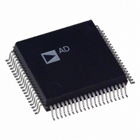
AD1843JS Analog Devices Inc, AD1843JS Datasheet - Page 28

AD1843JS
Manufacturer Part Number
AD1843JS
Description
IC CODEC STEREO 5V 16BIT 80PQFP
Manufacturer
Analog Devices Inc
Type
Stereo Audior
Datasheet
1.AD1843JS.pdf
(64 pages)
Specifications of AD1843JS
Rohs Status
RoHS non-compliant
Data Interface
Serial
Resolution (bits)
16 b
Number Of Adcs / Dacs
1 / 2
Sigma Delta
Yes
S/n Ratio, Adcs / Dacs (db) Typ
92 / 86
Dynamic Range, Adcs / Dacs (db) Typ
85 / 80
Voltage - Supply, Analog
4.75 V ~ 5.25 V
Voltage - Supply, Digital
2.85 V ~ 5.25 V
Operating Temperature
0°C ~ 70°C
Mounting Type
Surface Mount
Package / Case
80-MQFP, 80-PQFP
Available stocks
Company
Part Number
Manufacturer
Quantity
Price
Part Number:
AD1843JS
Manufacturer:
ADI/亚德诺
Quantity:
20 000
AD1843
This register is read only.
INIT
PDNO
ID3:0
res
This register is cleared to all “0” after any read or write access.
SU2
SU1
OVR1:0
Address 1
Address 0
Data 15
Data 15
Data 7
Data 7
INIT
res
res
res
ran out of samples. If this occurs, zeros are used in place of the unavailable data. This bit is “sticky” and is cleared
after any write to this register. It is also cleared by powering down DAC1 (see the DA1EN bit in Control Register
Address 27).
cleared to “00” after any write to this register. The peak amplitude as recorded by these bits is “sticky,” i.e., the larg-
est output magnitude recorded by these bits will persist until these bits are explicitly cleared. They are also cleared by
powering down the ADC right channel (see the ADREN bit in Control Register Address 27).
Clock Initialization Flag. This bit is set to “1” if the AD1843’s internal clocks generated from the crystal input pin
Revision Identification. These bits define the revision level of the AD1843. The first version of the AD1843 is
Reserved for future expansion. To ensure future compatibility, write “0” to all reserved bits.
ADC Right Overrange Detect. These bits record the largest output magnitude on the ADC right channel and are
XTALI have not yet stabilized. When set to “1,” Control Registers may be read if the AD1843 is configured as a Bus
Slave (see the definition for the BM pin), but Control Register writes will be blocked. This bit is set to a “1” after the
RESET pin is asserted, or when the power-down sequence (initiated by asserting the PWRDWN pin) has completed.
The bit is reset to “0” usually within 400 to 800 sec after the RESET or the PWRDWN pin is deasserted, depending
upon parasitic capacitance on the XTALI and XTALO pins outside the AD1843. Because these parasitics are a func-
tion of the board design and layout, the exact amount of time required for the crystal to start to oscillate, and the in-
ternal clocks to stabilize cannot be known exactly in advance.
Converter Power-Down Flag. This bit is set to “1” if the AD1843 conversion resources are powered down, or are in
the process of entering or exiting power down. Conversion resources are all resources in the AD1843 with the excep-
tion of the three clock generators and the serial interface. Conversion power-down is entered if either the power-down
pin (PWRDWN) is driven LO, or if the PDNI (Converter Power Down) bit in Control Register Address 28 is as-
serted. Power down is exited only if both pin (PWRDWN) and bit (PDNI) are deasserted. When this bit is set to
“1,” Control Registers may still be read, but only Control Registers 16–24, 26 and 28 which do not manage conver-
sion resources may be written. See the “Power Management” section for further details. This bit is set to “1” imme-
diately after a reset since the PDNI bit is initially asserted after a reset.
“0001.”
Initial default state after reset: 1100 0000 0000 0001 (C001 hex). Cleared to default and cannot be written to when:
the RESET pin is asserted LO; or when the PWRDWN pin is asserted LO.
DAC2 Sample Underrun. When set to “1,” this bit indicates that the four word stereo input buffer for DAC pair 2
ran out of samples. If this occurs, zeros are used in place of the unavailable data. This bit is “sticky” and is cleared
after any write to this register. It is also cleared by powering down DAC2 (see the DA2EN bit in Control Register
Address 27).
DAC1 Sample Underrun. When set to “1,” this bit indicates that the four word stereo input buffer for DAC pair 1
00 = Greater than –1.0 dB underrange
01 = Between –1.0 dB and 0 dB underrange
10 = Between 0 dB and 1 dB overrange
11 = Greater than 1.0 dB overrange
Data 14
Data 14
Data 6
PDNO
Data 6
res
res
res
Data 13
Data 13
Data 5
Data 5
res
res
res
res
Channel Status Flags
Codec Status and Revision Identification
Data 12
Data 12
Data 4
Data 4
res
res
res
res
–28–
Data 11
Data 11
Data 3
Data 3
OVR1
ID3
res
res
Data 10
Data 10
Data 2
Data 2
OVR0
ID2
res
res
Data 9
Data 1
Data 9
Data 1
OVL1
SU2
ID1
res
Data 8
Data 0
Data 8
Data 0
OVL0
SU1
ID0
res
REV. 0


