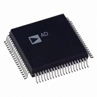
AD1843JS Analog Devices Inc, AD1843JS Datasheet - Page 33

AD1843JS
Manufacturer Part Number
AD1843JS
Description
IC CODEC STEREO 5V 16BIT 80PQFP
Manufacturer
Analog Devices Inc
Type
Stereo Audior
Datasheet
1.AD1843JS.pdf
(64 pages)
Specifications of AD1843JS
Rohs Status
RoHS non-compliant
Data Interface
Serial
Resolution (bits)
16 b
Number Of Adcs / Dacs
1 / 2
Sigma Delta
Yes
S/n Ratio, Adcs / Dacs (db) Typ
92 / 86
Dynamic Range, Adcs / Dacs (db) Typ
85 / 80
Voltage - Supply, Analog
4.75 V ~ 5.25 V
Voltage - Supply, Digital
2.85 V ~ 5.25 V
Operating Temperature
0°C ~ 70°C
Mounting Type
Surface Mount
Package / Case
80-MQFP, 80-PQFP
Available stocks
Company
Part Number
Manufacturer
Quantity
Price
Part Number:
AD1843JS
Manufacturer:
ADI/亚德诺
Quantity:
20 000
REV. 0
MNM4:0
ALLMM
MNOM
HPOM
HPOS
SUMM
DAC2T
DAC1T
res
LDA1GM
Address 9
LDA1GM
RDA1GM
Data 15
Data 7
Left and Right Mono Mix Gain/Attenuation Select. Least significant bit represents –1.5 dB.
00000 = +12.0 dB Gain
01000 = 0.0 dB
11111 = –34.5 dB Attenuation
All Mix Mute. Mutes all mixing (MIC, AUX1, AUX2, AUX3, and DAC2) to left and right DAC1, overriding the
independent mute control bits in Control Register Addresses 3 through 8.
0 = Mix to DAC1 Enabled
1 = Mix to DAC1 Muted
Mono Output Mute
0 = Mono Output Enabled
1 = Mono Output Muted
Headphone Output Mute (Left and Right)
0 = Headphone Output Enabled
1 = Headphone Output Muted
Headphone Output Voltage Swing (Left and Right)
0 = 2 volts peak-to-peak
1 = 4 volts peak-to-peak
Sum Left and Right Mute. Mutes mixing from SUML and SUMR pins to DAC1.
0 = SUML and SUMR Mix to DAC1 Enabled
1 = SUML and SUMR Mix to DAC1 Muted
DAC2 Gain/Attenuation Change Timing. This bit controls when changes to the DAC2 gain/attenuation setting
(Control Register 10) take effect. When set to “1,” changes take effect immediately. When reset to “0,” changes are
delayed until either the output level on DAC2 crosses zero (midscale), or until after a 10 to 12 ms time-out period is
reached. Delaying gain/attenuation changes until zero crossings reduces instantaneous output voltage changes, which
reduces audible “clicks.”
0 = Gain/Attenuation Changes Applied on Signal Zero Crossing or After a 10-12 ms Time-Out
1 = Gain/Attenuation Changes Applied Immediately
DAC1 Gain/Attenuation Change Timing. This bit controls when changes to the DAC1 gain/attenuation setting
(Control Register 9) take effect. When set to “1,” changes take effect immediately. When reset to “0,” changes are
delayed until either the output level on DAC1 crosses zero (midscale), or until after a 10 to 12 ms time-out period is
reached. Delaying gain/attenuation changes until zero crossings reduces instantaneous output voltage changes, which
reduces audible “clicks.”
0 = Gain/Attenuation Changes Applied on Signal Zero Crossing or After a 10-12 ms Time-Out
1 = Gain/Attenuation Changes Applied Immediately
Reserved for future expansion. To ensure future compatibility, write “0” to all reserved bits.
Initial default state after reset: 1000 1000 0110 1000 (8868 hex). Cleared to default and cannot be written to when:
the RESET pin is asserted LO; when the PWRDWN pin is asserted LO; or when the PDNO bit in Control Register
Address 0 is set to “1” (all conversions powered down). The MSB half (Data 15 through Data 8) of this Control Reg-
ister is cleared to default and cannot be written to also when: the AAMEN bit (analog input to analog mix disabled),
or the ANAEN bit (analog channels powered down) in Control Register 27 is reset to “0.”
Left DAC1 Analog Mute
0 = Left DAC1 Enabled
1 = Left DAC1 Muted
Data 14
Data 6
res
res
Output Control—DAC1 Analog Gain/Attenuation
LDA1G5
RDA1G5
Data 13
Data 5
LDA1G4
RDA1G4
Data 12
Data 4
–33–
LDA1G3
RDA1G3
Data 11
Data 3
LDA1G2
RDA1G2
Data 10
Data 2
LDA1G1
RDA1G1
Data 9
Data 1
LDA1G0
RDA1G0
Data 8
Data 0
AD1843


