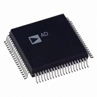
AD1843JS Analog Devices Inc, AD1843JS Datasheet - Page 46

AD1843JS
Manufacturer Part Number
AD1843JS
Description
IC CODEC STEREO 5V 16BIT 80PQFP
Manufacturer
Analog Devices Inc
Type
Stereo Audior
Datasheet
1.AD1843JS.pdf
(64 pages)
Specifications of AD1843JS
Rohs Status
RoHS non-compliant
Data Interface
Serial
Resolution (bits)
16 b
Number Of Adcs / Dacs
1 / 2
Sigma Delta
Yes
S/n Ratio, Adcs / Dacs (db) Typ
92 / 86
Dynamic Range, Adcs / Dacs (db) Typ
85 / 80
Voltage - Supply, Analog
4.75 V ~ 5.25 V
Voltage - Supply, Digital
2.85 V ~ 5.25 V
Operating Temperature
0°C ~ 70°C
Mounting Type
Surface Mount
Package / Case
80-MQFP, 80-PQFP
Available stocks
Company
Part Number
Manufacturer
Quantity
Price
Part Number:
AD1843JS
Manufacturer:
ADI/亚德诺
Quantity:
20 000
AD1843
DA1FLT
DAADR1:0
DAADL1:0
ADRFLT
ADLFLT
res
The table below lists the single path (DAC or ADC only) filter characteristics of the “Audio,” “Modem,” and “Resampler” digital
filters. Passband ripple and group delay must be doubled if the DAC is routed back through the ADC for digital resampling. For
further information, see the “Filter Selection” section and the filter frequency response plots, Figures 34 through 36.
Address 26
Data 15
DA2SM
Data 7
SCF
DAC1 (Left and Right Channels) Digital Filter Select. This bit is overridden when DRSFLT is set to “1.” See be-
Digital ADC Right Channel Source Select.
Digital ADC Left Channel Source Select.
ADC Right Channel Digital Filter Select and Analog Input Full Scale Mapping Select. Digital filter selected is over-
ADC Left Channel Digital Filter Select and Analog Input Full Scale Mapping Select. Digital filter selected is over-
Reserved for future expansion. To ensure future compatibility, write “0” to all reserved bits.
low for filter specifications. This bit can be altered only if DAC1 is powered down. Unlike DA2FLT, this bit does
not control the analog output swing of DAC1, which is fixed at 2.000 V p-p when the output level is set to 0 dB by
Control Register Address 9.
0 = Digital Audio Filter
1 = Digital Modem Filter
00 = Input from Analog: ADC Right Channel (Normal Operation)
01 = Reserved
10 = Input from Digital: DAC1 Right Channel (Digital Resampler)
11 = Input from Digital: DAC2 Right Channel (Digital Resampler)
00 = Input from Analog: ADC Left Channel (Normal Operation)
01 = Reserved
10 = Input from Digital: DAC1 Left Channel (Digital Resampler)
11 = Input from Digital: DAC2 Left Channel (Digital Resampler)
ridden when DRSFLT is set to “1.” See below for filter specifications. This bit can be altered only if the ADC right
channel is powered down.
0 = Digital Audio Filter. 2.800 V p-p analog input maps to 2
1 = Digital Modem Filter. 3.156 V p-p analog input maps to 2
ridden when DRSFLT is set to “1.” See below for filter specifications. This bit can be altered only if the ADC left
channel is powered down.
0 = Digital Audio Filter. 2.800 V p-p analog input maps to 2
1 = Digital Modem Filter. 3.156 V p-p analog input maps to 2
Initial default state after reset: 0000 0000 0000 0000 (0000 hex). Cleared to default and cannot be written to when:
the RESET pin is asserted LO; when the PWRDWN pin is asserted LO; or when the PDNO bit in Control Register
Address 0 is set to “1” (all conversions disabled).
Filter
Audio
Modem
Resampler
F
S
is the conversion (sample) rate.
Address 2).
Address 2).
Address 2).
Address 2).
Data 14
DA1SM
Data 6
FRS
Passband
Ripple
–0.016 dB
–0.220 dB
–0.035 dB
Codec Configuration—Serial Interface
Data 13
Data 5
FRST
res
Edge
0.400
0.442
0.400
Data 12
ADTLK
Data 4
res
F
F
F
S
S
S
–46–
Stopband
Ripple
< –91.8 dB
< –75.7 dB
< –92.2 dB
Data 11
ADRF1
DA2F1
Data 3
15
15
15
15
when gain is set to 0.0 dB (see Control Register
when gain is set to 0.0 dB (see Control Register
when gain is set to 0.0 dB (see Control Register
when gain is set to 0.0 dB (see Control Register
Data 10
ADRF0
DA2F0
Data 2
Edge
0.600
0.542
0.500
F
F
F
S
S
S
ADLF1
DA1F1
Data 9
Data 1
Linear
Group Delay
< 15/F
< 19/F
< 25/F
S
S
S
ADLF0
Data 8
DA1F0
Data 0
REV. 0


