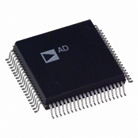
AD1843JS Analog Devices Inc, AD1843JS Datasheet - Page 54

AD1843JS
Manufacturer Part Number
AD1843JS
Description
IC CODEC STEREO 5V 16BIT 80PQFP
Manufacturer
Analog Devices Inc
Type
Stereo Audior
Datasheet
1.AD1843JS.pdf
(64 pages)
Specifications of AD1843JS
Rohs Status
RoHS non-compliant
Data Interface
Serial
Resolution (bits)
16 b
Number Of Adcs / Dacs
1 / 2
Sigma Delta
Yes
S/n Ratio, Adcs / Dacs (db) Typ
92 / 86
Dynamic Range, Adcs / Dacs (db) Typ
85 / 80
Voltage - Supply, Analog
4.75 V ~ 5.25 V
Voltage - Supply, Digital
2.85 V ~ 5.25 V
Operating Temperature
0°C ~ 70°C
Mounting Type
Surface Mount
Package / Case
80-MQFP, 80-PQFP
Available stocks
Company
Part Number
Manufacturer
Quantity
Price
Part Number:
AD1843JS
Manufacturer:
ADI/亚德诺
Quantity:
20 000
AD1843
5. Power up the clock generators and enable clock output
6. Configure conversion resources while they are in
Control Register readback (on the following frame) matches
the data written. Writes to Control Register Address 27 will
fail unless the conversion resources are out of power down.
pins. When the PDNI bit (Control Register Address 28, Bit
15) is reset to “0” in Step 4 above, the C3EN, C2EN,
C1EN, CONV[3:1], and BIT[3:1] bits, which are also lo-
cated in Control Register Address 28, may be set to “1” to
power up any clock generators which will be used, and to
enable any conversion clock and bit clock outputs needed.
While waiting for the conversion resources to enter standby,
it is convenient to write to the clock generator Control Regis-
ters (16 through 24) to select sample rates, bit clock frequen-
cies, external/internal sample rate lock mode, etc. This is
also a convenient time to write to Control Register Address
26 (if it was not already written in Step 3) to select the serial
interface configuration such as data format, SCLK fre-
quency, etc.
standby. Once in standby, the conversion resources may be
configured. They are forced to their defaults whenever pow-
ered down. Control Register Address 2 may be written to se-
lect between ADC sources and gain levels. Control Register
Address 15 may be written to select the assignments of
sample clock sources to conversion resource. Control Regis-
ter Addresses 13 and 14 may be written to enable digital data
flow paths which mix ADC output back into the DAC input.
Control Register Address 25 may be written to select conver-
sion resource filter mode (audio, modem or resampler), and
to select digital data flow paths which may be used to achieve
PWRDWN = LO
CONVERSION RESOURCES
ENTERING POWER DOWN
*
REGISTERS ARE ALWAYS READABLE, UNLESS RESET = LO
PWRDWN = HI
TIME: < 5ms
= STATE
= TRANSMISSION (WILL NOT BE INTERRUPTED ONCE STARTED UNLESS RESET = LO)
PDNO = 1
INIT = 0
PDNI = 1 OR
PWRDWN = LO
PWRDWN = LO
ADCL
STBY
EN
CONVERSION RESOURCES
POWER DOWN
ADCR
STBY
CONVERSION
RESOURCES
POWERED UP
RESET = LO
EN
ALL DOWN
AD1843 STATE
PDNO = 1
PDNO =1
PDNO = 0
INIT = 1
INIT = 0
INIT = 0
Figure 17. AD1843 Start-Up Sequence State Diagram
DAC1
STBY
EN
DAC2
STBY
CONVERSION RESOURCES
EN
PDNI = 1
EXITING POWER DOWN
ACEN = 0
PWRDWN = HI, RESET = HI
TIME: < 470ms
PDNI = 0
PDNO = 1
INIT = 0
TIME: 800µs?
INITIALIZING
PDNO = 1
INIT = 1
–54–
PDNI = 0
TIME: < 4ms
AUTOCAL
PDNO = 1
INIT = 0
7. Enable conversion resources. Conversion resources are
ACEN = 1
digital-to-digital sample rate conversion and DAC-to-DAC
digital mixing. Note that, with the exception of filter mode
and DAC-to-DAC digital mixing, all of these configuration
selections may also be changed while a conversion resource is
out of standby and enabled.
taken out of standby and enabled by writes to Control Regis-
ter Address 27. Control Register Address 27 contains indi-
vidual enable bits for the conversion resources which are
grouped as follows: DAC1 (stereo pair); DAC2 (stereo pair);
ADC left channel; ADC right channel; DAC2 to DAC1 mix;
and ADC input to DAC1 output mix.
If a DAC is enabled, it will begin requesting playback
samples on the next TDM frame (i.e., the DA2RQ and/or
the DA1RQ flags in the Status Register will be set to “1”).
Conversions will not actually begin until the first rising edge
of the conversion clock (assigned to the DAC) after the sixth
rising edge of the frame sync (SDFS) signal. This delay al-
lows the four word deep stereo FIFOs to be filled before con-
versions begin. (Six frames are required to fill a four word
deep FIFO because on the first frame, the DAC playback is
enabled; on the second frame, the DA2RQ and/or DA1RQ
flags are set to “1”; then four more frames are required to ac-
tually fill the FIFO.)
If an ADC is enabled, sampling of the analog input will be-
gin on the first rising edge of the conversion clock (assigned
to the ADC) after the sixth rising edge of the frame sync
(SDFS) signal. The data valid flags (ADRV and/or ADLV)
in the Status Word will be set to a “1,” indicating a sample is
being transmitted shortly thereafter. The exact TDM frame
INTERFACE: DOWN
CLOCK GENERATORS: DOWN
CONVERSIONS: DOWN
INTERFACE: READS ONLY IF SLAVE,
DOWN IF MASTER
CLOCK GENERATORS: DOWN
CONVERSIONS: DOWN
INTERFACE: ALIVE
CLOCK GENERATORS: ENABLEABLE
CONVERSIONS: DOWN
INTERFACE: ALIVE
CLOCK GENERATORS: ENABLEABLE
CONVERSIONS: DOWN
INTERFACE: ALIVE
CLOCK GENERATORS: ENABLEABLE
CONVERSIONS: ENABLEABLE
(CONTROL REGISTER ADDRESS 28)
(CONTROL REGISTER ADDRESS 28)
(CONTROL REGISTER ADDRESS 28)
(CONTROL REGISTER ADDRESS 27)
ACTIVITY LEVEL
NONE
NONE
POTENTIALLY ALL,
DEPENDING ON
ENABLED
RESOURCES
(SEE TEXT)
16-24, 26, 28
16-24, 26, 28
REGISTERS
WRITABLE
*
REV. 0


