AD1843JS Analog Devices Inc, AD1843JS Datasheet - Page 8
AD1843JS
Manufacturer Part Number
AD1843JS
Description
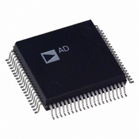
IC CODEC STEREO 5V 16BIT 80PQFP
Manufacturer
Analog Devices Inc
Type
Stereo Audior
Datasheet
1.AD1843JS.pdf
(64 pages)
Specifications of AD1843JS
Rohs Status
RoHS non-compliant
Data Interface
Serial
Resolution (bits)
16 b
Number Of Adcs / Dacs
1 / 2
Sigma Delta
Yes
S/n Ratio, Adcs / Dacs (db) Typ
92 / 86
Dynamic Range, Adcs / Dacs (db) Typ
85 / 80
Voltage - Supply, Analog
4.75 V ~ 5.25 V
Voltage - Supply, Digital
2.85 V ~ 5.25 V
Operating Temperature
0°C ~ 70°C
Mounting Type
Surface Mount
Package / Case
80-MQFP, 80-PQFP
Available stocks
Company
Part Number
Manufacturer
Quantity
Price

Part Number:
AD1843JS
Manufacturer:
ADI/亚德诺
Quantity:
20 000


AD1843
Serial Interface (Continued)
Pin Name
CS
TSO
TSI
XCTL[1:0]
PQFP
9
6
5
59, 58
AUX3R
AUX2R
AUX1R
AUX3L
AUX2L
AUX1L
GNDD
GNDD
SDFS
MICR
MICL
NC = NO CONNECT
SDO
TSO
V
V
MIN
V
BM
TSI
CS
NC
NC
NC
NC
DD
NC
DD
CC
10
11
12
13
14
15
16
17
18
19
20
21
22
23
24
25
1
2
3
4
5
6
7
8
9
TQFP
11
7
6
72, 74
100
26
99
27
98
28
97
29
96
30
I/O
I
O
I
I/O
95
31
94
32
Description
Chip Select. When CS is set HI, the serial interface I/O pins will be in their normal
active states. When CS is reset LO, SCLK, SDFS, and SDO are three-
stated; SCLK, SDFS and SDI inputs are ignored; and TSO drives out the logic
level received on TSI.
Time Slot Output. TSO is asserted HI by the AD1843 simultaneously with the LSB
of the last time slot used by the AD1843. It is used to daisy-chain multiple AD1843s
on a common TDM serial bus. If the power-down (PWRDWN) pin is asserted or if
the chip select pin (CS) is deasserted, TSO is set to the logic level on the TSI pin,
allowing powered-down or unselected AD1843s on a daisy-chain to be skipped.
Time Slot Input. Asserting TSI HI indicates to the AD1843 that it should use
the next six time slots beginning on the next SCLK period. It also enables TSO
to be asserted at the end of these six time slots. TSI is ignored (but should be tied
LO) when the AD1843 is the bus master since the bus master uses the first time
slots in a TDM frame.
External Control. These signals reflect the status of bits (Data 8 and 9) in Control
Register Address 28 of the AD1843. They may be used for signaling or controlling
external logic.
93
33
PIN CONFIGURATIONS
92
34
91
35
100-Lead TQFP
90
36
(Not to Scale)
89
37
AD1843
TOP VIEW
–8–
88
38
87
39
86
40
85
41
84
42
83
43
82
44
45
81
80
46
79
47
78
48
77
49
76
50
75
74
73
71
70
69
68
67
66
65
64
63
62
61
60
58
57
56
55
54
53
51
72
59
52
GNDD
XCTL1
NC
XCTL0
SYNC3
SYNC2
SYNC1
RESET
PWRDWN
NC
V
PDMNFT
NC
GNDA
HPOUTL
HPOUTC
HPOUTR
V
SUML
SUMR
NC
NC
GNDD
V
V
DD
DD
CC
CC
REV. 0
Related parts for AD1843JS
Image
Part Number
Description
Manufacturer
Datasheet
Request
R

Part Number:
Description:
±1.7g Dual-Axis IMEMS Accelerometer Evaluation Board
Manufacturer:
Analog Devices Inc
Datasheet:

Part Number:
Description:
Inertial Sensor Evaluation System
Manufacturer:
Analog Devices Inc
Datasheet:
Part Number:
Description:
Manufacturer:
Analog Devices Inc
Datasheet:
Part Number:
Description:
Manufacturer:
Analog Devices Inc
Datasheet:
Part Number:
Description:
Manufacturer:
Analog Devices Inc
Datasheet:
Part Number:
Description:
Manufacturer:
Analog Devices Inc
Datasheet:
Part Number:
Description:
Manufacturer:
Analog Devices Inc
Datasheet:
Part Number:
Description:
Manufacturer:
Analog Devices Inc
Datasheet:
Part Number:
Description:
Manufacturer:
Analog Devices Inc
Datasheet:
Part Number:
Description:
Manufacturer:
Analog Devices Inc
Datasheet:
Part Number:
Description:
Manufacturer:
Analog Devices Inc
Datasheet:
Part Number:
Description:
Manufacturer:
Analog Devices Inc
Datasheet:
Part Number:
Description:
Manufacturer:
Analog Devices Inc
Datasheet: