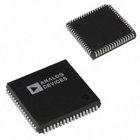
AD1845JP-REEL Analog Devices Inc, AD1845JP-REEL Datasheet - Page 32

AD1845JP-REEL
Manufacturer Part Number
AD1845JP-REEL
Description
IC CODEC STEREO 5V 16BIT 68PLCC
Manufacturer
Analog Devices Inc
Type
Stereo Audior
Datasheet
1.AD1845JP.pdf
(40 pages)
Specifications of AD1845JP-REEL
Rohs Status
RoHS non-compliant
Resolution (bits)
16 b
Number Of Adcs / Dacs
2 / 2
Sigma Delta
Yes
Dynamic Range, Adcs / Dacs (db) Typ
81 / 82
Voltage - Supply, Analog
4.75 V ~ 5.25 V
Voltage - Supply, Digital
4.75 V ~ 5.25 V
Operating Temperature
0°C ~ 70°C
Mounting Type
Surface Mount
Package / Case
68-PLCC
AD1845
POWER-UP AND RESET
The PWRDWN and RESET pin should be held in the active LO
state when power is first applied to the AD1845. The AD1845’s
initialization commences when PWRDWN and RESET have both
been deasserted (HI). While initializing, the AD1845 ignores all
writes and all reads will yield “1000 0000 (80h).” At the conclu-
sion of initialization, all registers will be set to their default values as
listed in Figure 5. When CDAK and PDAK are inactive during
power-up or reset, the conclusion of the initialization period,
after approximately 512 ms, can be detected by polling the
index register for some value other than “1000 0000 (80h).”
Upon power-up the AD1845 enters the Mode Change Enable
(MCE) state. In the default condition, the AD1845 expects to
receive a 24.576 MHz input clock source. To change the selec-
tion of the current or default input clock source, follow the steps
listed below:
• Wait for the AD1845 to initialize.
• Set the MODE2 bit to 1.
• Enter the MCE state, write to the Crystal/Clock Input Fre-
• The AD1845 will now resynchronize its internal states to the
• Clear the MCE bit.
ADVANCED POWER-DOWN MODES
The AD1845 has eight Advanced Power-Down Modes available
at any time. The user can control these power-down modes
through hardware by asserting the PWRDWN and RESET pins
or through software by writing to the Power-Down and the
Total Power-Down Control Registers. Figure 26 summarizes
the power-down delay, power-up delay, and power dissipation
for each power-down mode. A priority listing and description of
the power-down modes follows. Note that the hardware con-
trolled Power-Down and Reset modes take precedence over the
software controlled power-down states.
quency Select bits (XFS2:0) to select the desired frequency.
new clock. Writes to the AD1845 will be ignored. Poll the
index register for some value other than “1000 0000 (80h).”
Advanced
Power-Down
Mode
Operating
1. Power-Down
2. Reset
3. Total Power-Down
4. Standby
5. Mixer Power-Down HI
6. Mixer Only
7. ADC Power-Down
8. DAC Power-Down
“x” = Don’t Care
*Values shown are derived using a 24.576 MHz input clock source.
All values are proportional to the input clock source.
PWRDWN
Pin
LO
HI
HI
HI
HI
HI
HI
HI
RESET
Pin
HI
x
LO
HI
HI
HI
HI
HI
HI
Figure 26. Advanced Power-Down Mode Summary
TOTPWD ADCPWD DACPWD MIXPWD Power-Down
Bit
0
x
x
1
0
0
0
0
0
Bit
0
x
x
x
1
0
1
1
0
–32–
Bit
0
x
x
x
x
x
1
0
1
Hardware Controlled States
The hardware power-down states are accessed by bringing the
PWRDWN or RESET pin LO. Either of these signals place the
AD1845 into the maximum power conservation mode. Bringing
the PWRDWN or RESET pin HI will power-up the codec in
approximately 512 ms (see the Power-Up and Reset section of
this data sheet).
• Power-Down: PWRDWN immediately puts the AD1845 into
• Reset: RESET powers down the AD1845 gradually to its
Software Controlled States
To enter the Total Power-Down mode requires entering the
Mode Change Enable (MCE) state. After entering MCE, the
Total Power-Down mode can be accessed by writing a “1” to
the TOTPWD bit in the Total Power-Down Register. Exiting
the Total Power-Down mode (writing a “0” to the TOTPWD
bit in the Total Power-Down Register) will initialize the
AD1845 in approximately 512 ms (see the Power-Up and Reset
section of this data sheet).
• Total Power-Down: In the Total Power-Down mode the
To enter the software controlled power-down states in the
Power-Down Control Register, write a “1” to the control bits.
its lowest power-down state. The AD1845’s parallel inter-
face will not function and all bidirectional signal lines will be
in a high-impedance state.
lowest power-down state. The AD1845 performs a se-
quenced power-down that eliminates audible effects from the
DAC’s output. The XTAL1 input must be clocked for the
minimum duration of the RESET pulsewidth. The
AD1845’s parallel interface will not function and all bidirec-
tional signal lines will be in a high-impedance state. Note:
the clock must operate during the software or hardware
power-down process.
ADC, DAC, Mixer, and voltage reference are turned off,
but the digital interface remains active awaiting power-up.
All ADC and DAC data is flushed including data in the
capture and playback FIFOs.
Bit
0
x
x
x
1
1
0
0
0
Delay*
x
0 s
3 ms
3 ms
1/F
1/F
1/F
1/F
1/F
S
S
S
S
S
Power-Up
Delay*
x
512 ms
512 ms
512 ms
1/F
1/F
1/F
1/F
1/F
S
S
S
S
S
Power
Dissipation
600 mW
150 mW
180 mW
350 mW
260 mW
400 mW
425 mW
10 mW
10 mW
REV. C


