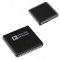
AD1845JP-REEL Analog Devices Inc, AD1845JP-REEL Datasheet - Page 7

AD1845JP-REEL
Manufacturer Part Number
AD1845JP-REEL
Description
IC CODEC STEREO 5V 16BIT 68PLCC
Manufacturer
Analog Devices Inc
Type
Stereo Audior
Datasheet
1.AD1845JP.pdf
(40 pages)
Specifications of AD1845JP-REEL
Rohs Status
RoHS non-compliant
Resolution (bits)
16 b
Number Of Adcs / Dacs
2 / 2
Sigma Delta
Yes
Dynamic Range, Adcs / Dacs (db) Typ
81 / 82
Voltage - Supply, Analog
4.75 V ~ 5.25 V
Voltage - Supply, Digital
4.75 V ~ 5.25 V
Operating Temperature
0°C ~ 70°C
Mounting Type
Surface Mount
Package / Case
68-PLCC
Parallel Interface
Pin Name
CDRQ
CDAK
PDRQ
PDAK
ADR1:0
RD
WR
CS
DATA7:0
DBEN
DBDIR
REV. C
PLCC TQFP
12
11
14
13
9 & 10 100 & 1
60
61
59
3–6 &
65–68
63
62
7
6
9
8
75
76
74
84–87 & I/O
90–93
78
77
I/O
O
I
O
I
I
I
I
I
O
O
Data Bus. These pins transfer data and control information between the codec and
Description
Capture Data Request. The assertion of this signal HI indicates that the codec has a cap-
tured audio sample from the ADC ready for transfer. This signal will remain asserted
until the internal capture FIFO is empty.
Capture Data Acknowledge. The assertion of this active LO signal indicates that the RD
cycle occurring is a DMA read from the capture buffer.
Playback Data Request. The assertion of this signal HI indicates that the codec is ready
for more DAC playback data. The signal will remain asserted until the internal playback
FIFO is full.
Playback Data Acknowledge. The assertion of this active LO signal indicates that the WR
cycle occurring is a DMA write to the playback buffer.
Codec Addresses. These address pins are asserted by the codec interface logic during a
control register/PIO access. The state of these address lines determine which direct
register is accessed.
Read Command Strobe. This active LO signal defines a read cycle from the codec. The
cycle may be a read from the control/PIO registers, or the cycles could be a read from
the codec’s DMA sample registers.
Write Command Strobe. This active LO signal indicates a write cycle to the codec. The
cycle may be a write to the control/PIO registers, or the cycle could be a write to the
codec’s DMA sample registers.
AD1845 Chip Select. The codec will not respond to any control/PIO cycle accesses
unless this active LO signal is LO. This signal is ignored during DMA transfers.
the host.
Data Bus Enable. This pin enables the external bus drivers. This signal is normally HI.
Data Bus Direction. This pin controls the direction of the data bus transceiver. HI
enables writes from the host bus to the AD1845; LO enables reads from the AD1845 to
the host bus. This signal is normally HI.
For control register/PIO cycles,
For DMA cycles,
For control register/PIO cycles,
For DMA cycles,
DBEN = (WR or RD) and CS
DBEN = (WR or RD) and (PDAK or CDAK).
DBDIR = RD and CS
DBDIR = RD and (PDAK or CDAK).
PIN FUNCTION DESCRIPTIONS
–7–
AD1845


