AD1849KP Analog Devices Inc, AD1849KP Datasheet - Page 19
AD1849KP
Manufacturer Part Number
AD1849KP
Description
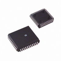
IC CODEC STEREO 5V 16BIT 44PLCC
Manufacturer
Analog Devices Inc
Type
Stereo Audior
Datasheet
1.AD1849KP.pdf
(28 pages)
Specifications of AD1849KP
Rohs Status
RoHS non-compliant
Data Interface
Serial
Resolution (bits)
16 b
Number Of Adcs / Dacs
2 / 2
Sigma Delta
Yes
Dynamic Range, Adcs / Dacs (db) Typ
83 / 86
Voltage - Supply, Analog
4.75 V ~ 5.25 V
Voltage - Supply, Digital
4.75 V ~ 5.25 V
Operating Temperature
0°C ~ 70°C
Mounting Type
Surface Mount
Package / Case
44-PLCC
Available stocks
Company
Part Number
Manufacturer
Quantity
Price

Part Number:
AD1849KP
Manufacturer:
ADI/亚德诺
Quantity:
20 000
Part Number:
AD1849KPZ
Manufacturer:
ADI/亚德诺
Quantity:
20 000


Daisy-Chaining Multiple Codecs
Up to four SoundPort Codecs can be daisy-chained with frame
sizes in multiples of 64 bits. The serial data is time-division
multiplexed (TDM), allocating each Codec its own 64-bit word
in the frame.
The pins that support TDM daisy-chaining of multiple Codecs
are the word chaining input (TSIN) and the word chaining out-
put (TSOUT). As described above, TSIN is used to indicate
the position of the first bit of a particular Codec’s 64-bit word
within the total frame.
The word chaining output (TSOUT) is generated by every Codec
during the transmission of the last bit of its 64-bit word. The
first device in any Codec chain uses an externally generated or
self-generated FSYNC signal as an input to TSIN. The TSOUT
of the first Codec is wired directly to the TSIN of the second
Codec and so on. The waveform of TSOUT is a pulse of one
SCLK period in duration. All Codecs share the same SCLK,
FSYNC, SDRX, and SDTX lines since they are selecting
different words from a common frame.
Note that a powered-down Codec immediately echoes TSIN on
TSOUT. Thus, a Codec can be added or removed from the
chain simply by using the PDN pin. See “Reset and Power
Down” below for more details. See Figure 9 for an illustration
of daisy-chained Codecs.
Note that at most, one Codec in a daisy-chain can be in master
mode without contention. All other Codecs must be in slave
mode, receiving SCLK and TSIN externally.
Each slave can use SCLK as its clock source. However, as an
alternative, it is possible to connect the CLKOUT pin of the
master Codec to the CLKIN pins of the slaves, so that the
sam-ple frequency selected by the master (from one of its two
crystals) will be automatically applied to the slaves. The master
must be programmed for the desired sample frequency and the
correct number of bits per frame. The slaves must be programmed
for CLKIN as the clock source, the correct number of bits per
EXTERNAL
DEVICE
FSYNC
RESET
SDRX
SCLK
SDTX
PDN2
PDN1
D/C
SCLK
SDRX
SDTX
FSYNC
TSIN
TSOUT
D/C
PDN
RESET
SCLK
SDRX
SDTX
FSYNC
TSIN
TSOUT
D/C
PDN
RESET
AD1849K #1
AD1849K #2
MASTER
SLAVE
CLKOUT
CLKIN
frame, and SCLK as an input. The slaves FSYNC out-puts will
be three-stated and thus can be connected to the master’s FSYNC
without contention.
If SCLK is the clock source, it must run at 256 × F
the frame size must be 256 bits, i.e., four words. By contrast, if
the master Codec’s CLKOUT is used as the clock source, then
it can run at either 256 × F
Parallel I/O Bits
Both Data and Control Words allocate Bit positions for “parallel
I/O,” PIO1:0. This provides a convenient mechanism for trans-
ferring signaling information between the serial data and control
streams and the external pair of bidirectional pins also named
“PIO1” and “PIO0.” The states of the parallel I/O bits and pins
do not affect the internal operation of the Codec in any way;
their exclusive use is for system signaling.
The PIO pins are open-drain and should be pulled HI externally.
They can be read (through serial output data) in either Control
or Data Mode and can be written (through serial input data) in
Data Mode exclusively. The values in the PIO field of the Control
Word serial input in Control Mode will be ignored. An external
device may drive either PIO pin LO even when written HI by
the Codec, since the pin outputs are open-drain. Thus, a PIO
value read back as a serial output bit may differ from the value
just written as a serial input bit.
The PIO pins are read on the rising edge of SCLK five (5) SCLK
periods before the first PIO bit is transmitted out over the serial
interface. In Data Mode, the PIO pins are sampled as Bit 20 starts
to be driven out. In Control Mode, the PIO pins are sampled
as Bit 36 starts being driven out. Timing para-meters are as
shown in Figure 7; PIO pin input data is relative to the rising
edge of SCLK. (Note that only the PIO pins are read on SCLK
rising edges.)
The PIO pins are driven very shortly after the PIO data bits in
the input Data Word are read (Data Mode only). They are driven
on the falling edge of SCLK (unlike any other output). The PIO
data bits in the input are located at Bits 15 and 14 in the Data
Word and at Bits 31 and 30 in the Control Word (Figure 8).
Due to the five (5) SCLK period delay, the PIO pins will be
driven out with new values for Data Mode on the SCLK falling
edge when Bit 8 is read in, and for Control Mode on the SCLK
falling edge when Bit 24 is read in.
CODEC STARTUP, MODES, AND TRANSITIONS
Reset and Power-Down
The AD1849K stereo codec can be reset by either of two closely
related digital input signals, RESET and Power-Down (PDN).
RESET is active LO and PDN is active HI. Asserting PDN is
equivalent to asserting RESET with two exceptions. First, if
PDN is asserted (when RESET is HI), then the TSIN and
TSOUT chaining pins remain active. TSOUT will immediately
echo whatever signal is applied to TSIN during power down.
This feature allows a very simple system test to detect “life”
even in a power-down state. It also allows the user to selectively
shut off codecs in a daisy chain by powering down the unwanted
codecs. The down-stream codecs will simply move up a word
position in frame. The second difference is that power consumption
will be lower in power-down mode than in exclusive reset mode.
The CMOUT and LOUT1C pins will not supply current while
the AD1849K is in the power-down state since all outputs
collapse to ground.
S
or 128 × F
S
.
AD1849K
S
, and therefore
Related parts for AD1849KP
Image
Part Number
Description
Manufacturer
Datasheet
Request
R

Part Number:
Description:
±1.7g Dual-Axis IMEMS Accelerometer Evaluation Board
Manufacturer:
Analog Devices Inc
Datasheet:

Part Number:
Description:
Inertial Sensor Evaluation System
Manufacturer:
Analog Devices Inc
Datasheet:
Part Number:
Description:
Manufacturer:
Analog Devices Inc
Datasheet:
Part Number:
Description:
Manufacturer:
Analog Devices Inc
Datasheet:
Part Number:
Description:
Manufacturer:
Analog Devices Inc
Datasheet:
Part Number:
Description:
Manufacturer:
Analog Devices Inc
Datasheet:
Part Number:
Description:
Manufacturer:
Analog Devices Inc
Datasheet:
Part Number:
Description:
Manufacturer:
Analog Devices Inc
Datasheet:
Part Number:
Description:
Manufacturer:
Analog Devices Inc
Datasheet:
Part Number:
Description:
Manufacturer:
Analog Devices Inc
Datasheet:
Part Number:
Description:
Manufacturer:
Analog Devices Inc
Datasheet:
Part Number:
Description:
Manufacturer:
Analog Devices Inc
Datasheet:
Part Number:
Description:
Manufacturer:
Analog Devices Inc
Datasheet: