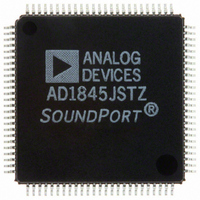
AD1845JSTZ Analog Devices Inc, AD1845JSTZ Datasheet - Page 11

AD1845JSTZ
Manufacturer Part Number
AD1845JSTZ
Description
IC CODEC AUDIO 5V 16BIT 100-TQFP
Manufacturer
Analog Devices Inc
Type
Stereo Audior
Datasheet
1.AD1845JP.pdf
(40 pages)
Specifications of AD1845JSTZ
Resolution (bits)
16 b
Number Of Adcs / Dacs
2 / 2
Sigma Delta
Yes
Dynamic Range, Adcs / Dacs (db) Typ
81 / 82
Voltage - Supply, Analog
4.75 V ~ 5.25 V
Voltage - Supply, Digital
4.75 V ~ 5.25 V
Operating Temperature
0°C ~ 70°C
Mounting Type
Surface Mount
Package / Case
100-TQFP, 100-VQFP
Lead Free Status / RoHS Status
Lead free / RoHS Compliant
Available stocks
Company
Part Number
Manufacturer
Quantity
Price
Company:
Part Number:
AD1845JSTZ
Manufacturer:
SYNCMOS
Quantity:
12 000
When 8-bit companding is specified, the ADCs’ linear output is
compressed to the format specified.
Note that all format conversions take place at input or output.
Internally, the AD1845 always uses 16-bit linear PCM represen-
tations to maintain maximum precision.
Timer Registers
The timer registers are provided for system level synchroniza-
tion, and for periodic interrupt generation. The 16-bit timer
time base is determined by the frequency of the connected input
clock source.
The timer is enabled by setting the Timer Enable bit, TE, in the
Alternate Feature Enable register. To set the timer, load the
Upper and Lower Timer Bits Registers. The timer value will
then be loaded into an internal count register with a value of
approximately 10 s (the exact timer value is listed in the regis-
ter descriptions). The internal count register will decrement
until it reaches zero, then the Timer Interrupt bit, TI, is set and
an interrupt will be sent to the host. The next timer clock will
load the internal count register with the value of the Timer
Register, and the timer will be reinitialized. To clear the inter-
rupt, write to the Status Register or write a “0” to TI.
Interrupts
The AD1845 supports interrupt conditions generated by DMA
playback count expiration, DMA capture count expiration, or
timer expiration. The INT bit will remain set, HI, until a write
has been completed to the Status Register or by clearing the TI,
CI, or PI bit (depending on the existing condition) in the Cap-
ture Playback Timer Register. The IEN bit of the Pin Control
Register determines whether the interrupt pin responds to an
interrupt condition and reflects the interrupt state on the
INT status bit.
REV. C
COMPRESSION
COMPRESSED
Figure 3.
TRUNCATION
ADC OUTPUT
INPUT DATA
EXPANSION
Figure 2.
DAC INPUT
15
15
15
15
15
15
-Law or A-Law Compression
MSB
MSB
MSB
MSB
MSB
MSB
-Law or A-Law Expansion
LSB
LSB
8 7
8 7
0 0 0 0 0 0 0 0
LSB
LSB
3/2
3/2
LSB
3/2
2/1
0 0 0 / 0 0
2/1
2/1
LSB
0
0
0
0
0
0
–11–
Power Supplies and Voltage Reference
The AD1845 operates from a +5 V power supply. Independent
analog and digital supplies are recommended for optimal perfor-
mance though excellent results can be obtained in single-supply
systems. A voltage reference is included on the codec and its
2.25 V buffered output is available on an external pin (V
The reference output can be used for biasing op amps used in
dc coupling. The internal reference is externally bypassed to
analog ground at the V
Clocks and Sample Rates
The AD1845 operates from a single external crystal or clock
source. From a single input, a wide range of sample rates can be
generated. The AD1845 default frequency source is a
24.576 MHz input. The AD1845 can also be driven from a
14.31818 MHz (OSC), 24 MHz, 25 MHz or 33 MHz input
frequency source. In MODE1, the input drives the internal
variable sample frequency generator to derive the following
AD1848 compatible sample rates: 5.5125, 6.615, 8, 9.6,
11.025, 16, 18.9, 22.05, 27.42857, 32, 33.075, 37.8, 44.1,
48 kHz. In MODE2, the AD1845 can be programmed to gen-
erate any sample frequency between 4 kHz and 50 kHz with
1 Hz resolution. Note that it is no longer required to enter
Mode Change Enable (MCE) to change the sample rate. This
feature allows the user to change the AD1845’s sample rate “on
the fly.”
CONTROL REGISTERS
Control Register Architecture
The AD1845 SoundPort Stereo Codec accepts both data and
control information through its byte-wide parallel port. Indirect
addressing minimizes the number of external pins required to
access all 37 of its byte-wide internal registers. Only two exter-
nal address pins, ADR1:0, are required to accomplish all data
and control transfers. These pins select one of five direct regis-
ters. (ADR1:0 = 3 addresses two registers, depending on
whether the transfer is for a playback or capture.)
ADR1:0
0
1
2
3
Figure 4. Direct Register Map
REF_F
Register Name
Index Address Register
Indexed Data Register
Status Register
PIO Data Register
pin.
AD1845
REF
).


