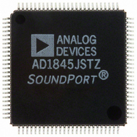
AD1845JSTZ Analog Devices Inc, AD1845JSTZ Datasheet - Page 14

AD1845JSTZ
Manufacturer Part Number
AD1845JSTZ
Description
IC CODEC AUDIO 5V 16BIT 100-TQFP
Manufacturer
Analog Devices Inc
Type
Stereo Audior
Datasheet
1.AD1845JP.pdf
(40 pages)
Specifications of AD1845JSTZ
Resolution (bits)
16 b
Number Of Adcs / Dacs
2 / 2
Sigma Delta
Yes
Dynamic Range, Adcs / Dacs (db) Typ
81 / 82
Voltage - Supply, Analog
4.75 V ~ 5.25 V
Voltage - Supply, Digital
4.75 V ~ 5.25 V
Operating Temperature
0°C ~ 70°C
Mounting Type
Surface Mount
Package / Case
100-TQFP, 100-VQFP
Lead Free Status / RoHS Status
Lead free / RoHS Compliant
Available stocks
Company
Part Number
Manufacturer
Quantity
Price
Company:
Part Number:
AD1845JSTZ
Manufacturer:
SYNCMOS
Quantity:
12 000
AD1845
DIRECT CONTROL REGISTER DEFINITIONS
IXA4:0
TRD
MCE
INIT
Immediately after reset and once the AD1845 has left the INIT state, the initial value of this register will be “0100 0000 (40h).”
During AD1845 initialization, this register cannot be written and always reads “1000 0000 (80h).”
IXD7:0
During AD1845 initialization, this register cannot be written and always reads as “1000 0000 (80h).”
Index Address Register (ADR1:0 = 0)
Indexed Data Register (ADR1:0 = 1)
ADR1:0
ADR1:0
0
1
Index Address. These bits define the address of the AD1845 register accessed by the Indexed Data Register.
These bits are read/write. IXA4 is not active in MODE1. Always write 0 to this bit when using the AD1845 in
MODE1.
Transfer Request Disable. This bit, when set, causes PIO and DMA transfers to cease when the Interrupt Status
(INT) bit of the Status Register is set.
0
1
Mode Change Enable. This bit must be set whenever the current functional mode of the AD1845 is changed
where noted in the Indirect Control Registers 8, 9, 28 and 29. MCE must be cleared at the completion of the
desired register changes.
The DAC outputs are automatically muted when the MCE bit is set. After MCE is cleared, the DAC outputs will
be restored to the state specified by the LDM and RDM mute bits.
Both ADCs and DACs are automatically muted for 32 sample cycles after exiting the MCE state to allow the refer-
ence and all filters to settle. The ADCs will produce midscale values; the DACs’ analog output will be muted. All
converters are internally operating during these 32 sample cycles, and the AD1845 will expect playback data and
will generate (midscale) capture data. Note that the autocalibrate-in-progress (ACI) bit will be set on exiting from
the MCE state only when ACAL is set. If ACAL bit is set, ACI will remain HI for these 384 sample cycles, allow-
ing system software to poll this bit rather than count cycles.
Special sequences must be followed if autocalibrate (ACAL) is set during mode change enable. See the
“Autocalibration” section.
AD1845 Initialization. This bit is set when the AD1845 cannot respond to parallel bus cycles. This bit is
read-only.
Register.
Indexed Register Data. These bits contain the contents of the AD1845 register referenced by the Indexed Data
Transfers Enabled During Interrupt. PDRQ and CDRQ pin outputs are generated uninhibited by interrupts.
DMA Current Counter Register decrements with every sample transferred when either PEN or CEN are enabled.
Transfers Disabled By Interrupt. PDRQ and CDRQ pin outputs are generated only if INT bit is 0 (when
either PEN or CEN, respectively are enabled). Any pending playback or capture requests are allowed to
complete at the time when INT is set. After pending requests complete, the data in the FIFO will be con-
sumed at the sample rate. Subsequently, the midscale inputs will be internally generated for the DACs if
the DACZ bit is set, otherwise, the previous valid sample will be repeated, and the ADC output buffer will
contain the last valid output. Clearing the sticky INT bit (or the TRD bit) will cause the resumption of
playback and/or capture requests (presuming PEN and/or CEN are enabled). The DMA Current Counter
Register will not decrement while both the TRD bit is set and the INT bit is a one. No over run or under
run error will be reported when transfers are disabled by INT.
Data 7
Data 7
IXD7
INIT
Data 6
Data 6
MCE
IXD6
Data 5
Data 5
IXD5
TRD
Data 4
–14–
Data 4
IXA4
IXD4
Data 3
Data 3
IXA3
IXD3
Data 2
Data 2
IXA2
IXD2
Data 1
Data 1
IXA1
IXD1
Data 0
Data 0
IXA0
IXD0
REV. C


