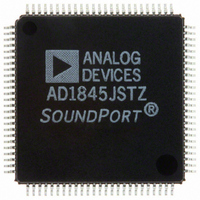
AD1845JSTZ Analog Devices Inc, AD1845JSTZ Datasheet - Page 16

AD1845JSTZ
Manufacturer Part Number
AD1845JSTZ
Description
IC CODEC AUDIO 5V 16BIT 100-TQFP
Manufacturer
Analog Devices Inc
Type
Stereo Audior
Datasheet
1.AD1845JP.pdf
(40 pages)
Specifications of AD1845JSTZ
Resolution (bits)
16 b
Number Of Adcs / Dacs
2 / 2
Sigma Delta
Yes
Dynamic Range, Adcs / Dacs (db) Typ
81 / 82
Voltage - Supply, Analog
4.75 V ~ 5.25 V
Voltage - Supply, Digital
4.75 V ~ 5.25 V
Operating Temperature
0°C ~ 70°C
Mounting Type
Surface Mount
Package / Case
100-TQFP, 100-VQFP
Lead Free Status / RoHS Status
Lead free / RoHS Compliant
Available stocks
Company
Part Number
Manufacturer
Quantity
Price
Company:
Part Number:
AD1845JSTZ
Manufacturer:
SYNCMOS
Quantity:
12 000
AD1845
The PIO Data Registers are two registers mapped to the same address. Writes send data to the PIO Playback Data Register
(PD7:0). Reads will receive data from the PIO Capture Data Register (CD7:0).
During AD1845 initialization, the PIO Playback Data Register cannot be written to and the Capture Data Register is always read
as “1000 0000 (80h).”
CD7:0
PD7:0
INDIRECT CONTROL REGISTER DEFINITIONS
The following control registers are accessed by writing index values to IXA3:0 in the Index Address Register (ADR1:0 = 0) followed
by a read/write to the Indexed Data Register (ADR1:0 = 1).
LIG3:0
res
LMGE
LSS1:0
This register’s initial state after reset is “000x 0000.”
RIG3:0
res
RMGE
RSS1:0
PIO Data Registers (ADR1:0 = 3)
Right Input Control (IXA3:0 = 1)
Left Input Control (IXA3:0 = 0)
ADR1:0
IXA3:0
IXA3:0
3
3
1
0
PIO Capture Data Register. This is the control register where capture data is read during programmed I/O data
transfers.
The reading of this register will increment the capture byte state machine so that the following read will be from
the next appropriate byte in the sample. The exact byte which is next to be read can be determined by reading the
Status Register. Once all relevant bytes have been read, the state machine will stay pointed to the last byte of the
sample until a new sample is received from the ADCs. Once this has occurred, the state machine and Status
Register will point to the first byte of the sample.
PIO Playback Data Register. This is the control register where playback data is written during programmed I/O
data transfers.
Writing data to this register will increment the playback byte tracking state machine so that the following write will
be to the correct byte of the sample. Once all bytes of a sample have been written, subsequent byte writes to this
port are ignored. The state machine is reset when the current sample is sent to the DACs.
LSS1
0
0
1
1
Right Input Gain Select. The least significant bit of this gain select represents +1.5 dB. Maximum gain is +22.5 dB.
Reserved for future expansion. Always write a zero to this bit.
Right Input Microphone Gain Enable. This bit will enable the +20 dB gain of the right MIC input signal.
Right Input Source Select. These bits select the input source for the right channel gain stage preceding the right
ADC.
Left input gain select. The least significant bit of this gain select represents +1.5 dB. Maximum gain is +22.5 dB.
Reserved for future expansion. Always write a zero to this bit.
Left Input Microphone Gain Enable. This bit will enable the +20 dB gain of the left MIC input signal.
Left Input Source Select. These bits select the input source for the left gain stage preceding the left ADC.
Data 7
Data 7
Data 7
RSS1
CD7
PD7
LSS1
LSS0
0
1
0
1
Left Input Source
Left Line Source Selected
Left Auxiliary 1 Source Selected
Left Microphone Source Selected
Left Line Post-Mixed DAC Output Source Selected
Data 6
Data 6
Data 6
RSS0
CD6
PD6
LSS0
RMGE
Data 5
Data 5
Data 5
LMGE
CD5
PD5
–16–
Data 4
Data 4
Data 4
CD4
PD4
res
res
Data 3
Data 3
Data 3
RIG3
CD3
PD3
LIG3
Data 2
Data 2
Data 2
RIG2
CD2
PD2
LIG2
Data 1
Data 1
Data 1
RIG1
CD1
PD1
LIG1
Data 0
Data 0
Data 0
RIG0
CD0
LIG0
PD0
REV. C


