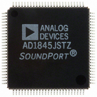
AD1845JSTZ Analog Devices Inc, AD1845JSTZ Datasheet - Page 31

AD1845JSTZ
Manufacturer Part Number
AD1845JSTZ
Description
IC CODEC AUDIO 5V 16BIT 100-TQFP
Manufacturer
Analog Devices Inc
Type
Stereo Audior
Datasheet
1.AD1845JP.pdf
(40 pages)
Specifications of AD1845JSTZ
Resolution (bits)
16 b
Number Of Adcs / Dacs
2 / 2
Sigma Delta
Yes
Dynamic Range, Adcs / Dacs (db) Typ
81 / 82
Voltage - Supply, Analog
4.75 V ~ 5.25 V
Voltage - Supply, Digital
4.75 V ~ 5.25 V
Operating Temperature
0°C ~ 70°C
Mounting Type
Surface Mount
Package / Case
100-TQFP, 100-VQFP
Lead Free Status / RoHS Status
Lead free / RoHS Compliant
Available stocks
Company
Part Number
Manufacturer
Quantity
Price
Company:
Part Number:
AD1845JSTZ
Manufacturer:
SYNCMOS
Quantity:
12 000
Switching between playback and capture in Single-Channel
DMA mode does not require changing the PPIO and CPIO bits
or passing through the Mode Change Enable state except for
initial setup. For setup, assign zeros to both PPIO and CPIO.
This configures both playback and capture for DMA. Following
setup, switching between playback and capture can be effected
entirely by setting and clearing the PEN and CEN control bits,
a technique which avoids having to enter Mode Change Enable.
Dual-Channel DMA
The AD1845 is designed to support full duplex DMA operation
by allowing simultaneous capture and playback. The Dual-
Channel DMA feature enables playback and capture DMA
requests and acknowledges to occur on separate DMA channels.
Capture and playback are enabled and set for DMA transfers.
In addition, Dual-Channel DMA must be set (SDC = 0). It is
not necessary to enter MCE (Mode Change Enable) to change
PEN and CEN (Playback and Capture Enable).
DMA Timing
Below, timing parameters are shown for 8-Bit Mono Sample
Read/Capture and Write/Playback DMA transfers in Figures 22
and 23. The same timing parameters apply to multi-byte trans-
fers. The relationship between timing signals is shown in Fig-
ures 24 and 25.
The Host Interrupt Pin (INT) will go HI after a sample transfer
in which the Current Count Register underflows.
REV. C
DBDIR OUTPUT
DBEN & DBDIR
DBEN OUTPUT
ISA BUS BCLK
CDRQ OUTPUT
ISA BUS BCLK
PDRQ OUTPUT
CDAK INPUT
PDAK INPUT
Figure 23. 8-Bit Mono DMA Write/Playback Cycle
Figure 22. 8-Bit Mono DMA Read/Capture Cycle
WR INPUT
OUTPUTS
RD INPUT
OUTPUTS
OUTPUTS
DATA7:0
DATA7:0
HI
t
DBDL
t
DSDL
t
t
DKSU
DKSU
t
RDDV
t
t
t
DRHD
DRHD
WDSU
t
t
STW
STW
t
t
t
DHD2
DKHDb
DKHDa
t
DHD1
–31–
DMA Interrupt
Writing to the internal 16-bit Base Count Register sets up the
count value for the number of samples to be transferred. Note
that the number of bytes transferred for a given count will be a
function of the selected global data format. The internal Cur-
rent Count Register is updated with the current contents of the
Upper and Lower Base Count Registers when a write occurs to
the Upper Base Count Register.
The Current Count Register cannot be read by the host. Read-
ing the Base Count Registers will only read back the initializa-
tion values written to them.
The Current Count Register decrements by one after every
sample transferred. An interrupt event is generated after the
Current Count Register is zero and an additional playback
sample is transferred. The INT bit in the Status Register always
reflects the current internal interrupt state defined above. The
external INT pin will only go active HI if the Interrupt Enable
(wIEN) bit in the Interface Configuration Register is set. If the
IEN bit is zero, the external INT pin will always stay LO, even
though the Status Register’s INT bit may be set.
ISA BUS BCLK
ISA BUS BCLK
CDRQ /PDRQ
CDRQ /PDRQ
CDAK/PDAK
CDAK/PDAK
RD OR WR
Figure 24. 8-Bit Stereo or 16-Bit Mono DMA Cycle
RD OR WR
OUTPUTS
OUTPUTS
DATA7:0
DATA7:0
INPUTS
INPUTS
INPUTS
INPUTS
Figure 25. 16-Bit Stereo DMA Interrupt
BYTE
LOW
SAMPLE
LEFT
t
BWDN
LOW BYTE
LEFT/
BYTE
HIGH
t
BWDN
BYTE
LOW
AD1845
SAMPLE
RIGHT
HIGH BYTE
RIGHT/
BYTE
HIGH


