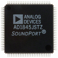
AD1845JSTZ Analog Devices Inc, AD1845JSTZ Datasheet - Page 35

AD1845JSTZ
Manufacturer Part Number
AD1845JSTZ
Description
IC CODEC AUDIO 5V 16BIT 100-TQFP
Manufacturer
Analog Devices Inc
Type
Stereo Audior
Datasheet
1.AD1845JP.pdf
(40 pages)
Specifications of AD1845JSTZ
Resolution (bits)
16 b
Number Of Adcs / Dacs
2 / 2
Sigma Delta
Yes
Dynamic Range, Adcs / Dacs (db) Typ
81 / 82
Voltage - Supply, Analog
4.75 V ~ 5.25 V
Voltage - Supply, Digital
4.75 V ~ 5.25 V
Operating Temperature
0°C ~ 70°C
Mounting Type
Surface Mount
Package / Case
100-TQFP, 100-VQFP
Lead Free Status / RoHS Status
Lead free / RoHS Compliant
Available stocks
Company
Part Number
Manufacturer
Quantity
Price
Company:
Part Number:
AD1845JSTZ
Manufacturer:
SYNCMOS
Quantity:
12 000
Figure 30 shows ac-coupled line outputs. The resistors are used
to center the output signals around analog ground. If dc-cou-
pling is desired, V
above, if desired.
A circuit for headphone drive is illustrated in Figure 31. Drive is
supplied by +5 V operational amps. The circuit shown ac
couples the headphones to the line output.
Figure 32 illustrates reference bypassing. V
connected to its bypass capacitors.
Figure 33 illustrates signal-path filtering capacitors, L_FILT
and R_FILT. The AD1845 must use 1.0 F capacitors; the
AD1845 will not perform properly with 1000 pF capacitors.
The 1.0 F capacitors required by the AD1845 can be of any
type.
The crystal shown in the crystal connection circuitry of Fig-
ure 34 should be 24.576 MHz, fundamental-mode and parallel-
tuned. Note that using the exact data sheet frequencies is not
required and that external clock sources can be used to over-
drive the AD1845’s internal oscillators. (See the description of
the CFS2:0 control bits above.) If using an external clock source,
apply it to the crystal input pins while leaving the crystal output
pins unconnected. Attention should be paid to providing low
jitter external input clocks.
REV. C
Figure 33. External Filter Capacitor Connections
Figure 31. Headphone Drive Connections
Figure 32. Voltage Reference Bypassing
R_OUT
L_OUT
V_REF
V
REF_F
Figure 30. Line Output Connections
1.0µF
R_OUT
L_OUT
REF
10k
10k
could be used with op amps as mentioned
1.0µF
L_FILT
SSM-2135
10µF
1 F
1 F
8.66k
8.66k
1.0µF
R_FILT
47k
47k
470 F
470 F
V
REF
REF_F
HEADPHONE
LEFT
HEADPHONE
RIGHT
should only be
10µF
–35–
Note: XTAL2I and XTAL2O, are not used in the AD1845.
Analog Devices also recommends a pull-down resistor for
PWRDWN.
Good, standard engineering practices should be applied for
power-supply decoupling. Decoupling capacitors should be
placed as close as possible to package pins. If a separate analog
power supply is not available, we recommend the circuit shown
in Figure 35 for using a single +5 V supply. Ferrite beads suffice
for the inductors shown (typically 600
circuitry should be as close to the supply pins as is practical.
GROUNDING AND LAYOUT
Analog Devices recommends a split ground plane as shown in
Figure 36. The analog plane and the digital plane are connected
directly under the AD1845. Splitting the ground plane directly
under the SoundPort Codec is optimal because analog pins will
be located above the analog ground plane and digital pins will
be located directly above the digital ground plane for the best
isolation.
Other schemes may also yield satisfactory results. If the split
ground plane recommended here is not possible, the AD1845
should be entirely over the analog ground plane with the op-
tional 74_245 transceiver over the digital plane.
Some manufacturers of compatible devices differentiate between
digital supply pins used to power internal logic and digital sup-
ply pins used to power the ISA bus driver. Their recommended
layout suggests connecting the internal logic supply pins to the
analog supply. A potential problem can occur if the layout con-
nects digital supply pins to the analog supply. Connecting some
of the digital supply pins to one supply and some of the digital
supply pins to a different supply can create an internal short
between the two different +5 V supplies.
Figure 35. Recommended Power Supply Bypassing
SUPPLY
+5V
10 F –
+
Figure 34. Crystal Connections
0.1 F
20–64pF
0.1 F
XTAL1I
FB
FB
24.576 MHz
+
–
+
10 F
–
10 F
XTAL1O
V
CC
V
V
at 100 MHz). This
20–64pF
DD
DD
0.1 F
0.1 F
0.1 F
AD1845
V
DD
0.1 F
0.1 F
V
CC


