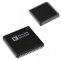
AD1845JPZ Analog Devices Inc, AD1845JPZ Datasheet - Page 8

AD1845JPZ
Manufacturer Part Number
AD1845JPZ
Description
IC CODEC STEREO 5V 16BIT 68PLCC
Manufacturer
Analog Devices Inc
Type
Stereo Audior
Datasheet
1.AD1845JP.pdf
(40 pages)
Specifications of AD1845JPZ
Resolution (bits)
16 b
Number Of Adcs / Dacs
2 / 2
Sigma Delta
Yes
Dynamic Range, Adcs / Dacs (db) Typ
81 / 82
Voltage - Supply, Analog
4.75 V ~ 5.25 V
Voltage - Supply, Digital
4.75 V ~ 5.25 V
Operating Temperature
0°C ~ 70°C
Mounting Type
Surface Mount
Package / Case
68-PLCC
Single Supply Voltage (typ)
5V
Single Supply Voltage (min)
4.75V
Single Supply Voltage (max)
5.25V
Package Type
PLCC
Lead Free Status / RoHS Status
Lead free / RoHS Compliant
AD1845
Analog Signals
Pin Name
L_LINE
R_LINE
L_MIC
R_MIC
L_AUX1
R_AUX1
L_AUX2
R_AUX2
L_OUT
R_OUT
M_IN
M_OUT
Miscellaneous
Pin Name
XTAL1I
XTAL1O
XTAL2I
XTAL2O
PWRDWN
INT
XCTL1:0
RESET
V
V
L_FILT
R_FILT
NC
REF
REF_F
PLCC TQFP
30
27
29
28
39
42
38
43
40
41
46
47
PLCC TQFP
17
18
21
22
23
57
58 & 56 73 & 71
24
32
33
31
26
48–52, 2–5, 21–24
55
31
28
30
29
45
48
44
49
46
47
56
57
12
13
16
17
18
72
19
35
38
33
25
26, 27, 32, 34,
36, 37, 39,
50–53, 58–66,
69, 70, 80–83,
94–97
I/O
I
I
I
I
I
I
I
I
O
O
I
O
I/O
I
O
I
O
O
I
O
I
I
I
Description
Left Line Input.
Right Line Input.
Left Microphone Input. This signal can be either line level or –20 dB from line level
(using the on-chip 20 dB gain block).
Right Microphone Input. This signal can be either line level or –20 dB from line level
(using the on-chip 20 dB gain block).
Left Auxiliary #1 Line Input.
Right Auxiliary #1 Line Input.
Left Auxiliary #2 Line Input.
Right Auxiliary #2 Line Input.
Left Line Output.
Right Line Output.
Mono Input.
Mono Output.
Description
24.576 MHz Crystal #1 Input.
24.576 MHz Crystal #1 Output.
Not used on the AD1845.
Not used on the AD1845.
Power Down Signal. Active LO places the AD1845 in its lowest power consumption
mode. All sections of the AD1845, including the digital interface, are shut down and
consume minimal power.
Host Interrupt Pin. A host interrupt is generated to notify the host that a specified
event has occurred.
External Control. These signals reflect the current status of register bits inside the
AD1845. They can be used for signaling or to control external logic.
Reset. Active LO resets all digital registers and filters, and resets all analog filters. Active
LO places the AD1845 in the lowest power consumption mode. XTAL1 is required to be
running during the minimum low pulsewidth of the reset signal.
Voltage Reference. Nominal 2.25 volt reference available for dc-coupling and level-
shifting. V
Voltage Reference Filter. Voltage reference filter point for external bypassing only.
Left Channel Filter. This pin requires a 1.0 F capacitor to analog ground for proper
operation.
Right Channel Filter. This pin requires a 1.0 F capacitor to analog ground for proper
operation.
No Connect.
REF
should not be used to sink or source current.
–8–
REV. C


