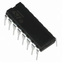
ETC5054N/H STMicroelectronics, ETC5054N/H Datasheet - Page 5

ETC5054N/H
Manufacturer Part Number
ETC5054N/H
Description
IC CODEC/FILTER SERIAL 16-DIP
Manufacturer
STMicroelectronics
Type
PCM Codec/Filterr
Datasheet
1.ETC5054N-XH.pdf
(18 pages)
Specifications of ETC5054N/H
Data Interface
Serial
Resolution (bits)
8 b
Number Of Adcs / Dacs
1 / 2
Sigma Delta
No
Voltage - Supply, Analog
4.75 V ~ 5.25 V
Operating Temperature
-25°C ~ 125°C
Mounting Type
Through Hole
Package / Case
16-DIP (0.300", 7.62mm)
Lead Free Status / RoHS Status
Lead free / RoHS Compliant
Other names
497-1339-5
Available stocks
Company
Part Number
Manufacturer
Quantity
Price
edges clock out the remaining seven bits. The D
output is disabled by the falling BCLK
lowing the eighth rising edge, or by FS
low, which-ever comes later. A rising edge on the
receive frame sync pulse, FS
PCM data at D
falling edges of BCLK
mode). Both devices may utilize the long frame
sync pulse in synchronous or asynchronous
mode.
TRANSMIT SECTION
The transmit section input is an operational ampli-
fier with provision for gain adjustment using two
external resistors, see figure 6. The low noise and
wide bandwidth allow gains in excess of 20 dB
across the audio passband to be realized. The op
amp drives a unitygain filter consisting of RD ac-
tive pre-filter, followed by an eighth order
switched-capacitor bandpass filter clocked at 256
kHz. The output of this filter directly drives the en-
coder sample-and-hold circuit. The A/D is of com-
panding type according to A-law (ETC5057) or –
law (ETC5054) coding conventions. A precision
voltage reference is trimmed in manufacturing to
provide an input overload (t
peak (see table of transmission characteristics).
The FS
of the filter output, and then the successive-ap-
ABSOLUTE MAXIMUM RATINGS
ELECTRICAL OPERATING CHARACTERISTICS V
T
are referenced to GNDA.
Symbol
A
V
Symbol
V
V
IN
= 0 C to 70 C; Typical Characteristics Specified at V
V
V
I
I
I
OZ
T
OH
IH
OL
IL
V
V
, V
IH
T
IL
oper
CC
BB
stg
OUT
X
frame sync pulse controls the sampling
Input Low Voltage
Input High Voltage
Output Low Voltage
I
I
Output High Voltage
I
Input Low Current (GNDA
Input High Current (V
Output Current in HIGH Impedance State (TRI-STATE)
(GNDA
L
L
H
= 3.2mA
= 3.2mA, Open Drain
= 3.2mA
V
V
Voltage at any Analog Input or Output
Voltage at Any Digital Input or Output
Operating Temperature Range
Storage Temperature Range
Lead Temperature (soldering, 10 seconds)
CC
BB
R
to be latched in on the next eight
to GNDA
to GNDA
V
O
R
V
CC
(BCLK
)
MAX
IH
) of nominally 2.5V
R
X
V
, will cause the
IN
in synchronous
V
Parameter
IN
V
Parameter
CC
X
V
) except BCLK
edge fol-
IL
X
, all digital inputs)
going
X
CC
R
/BCLKSEL
proximation encoding cycle begins. The 8-bit
code is then loaded into a buffer and shifted out
through D
coding delay will be approximately 165 s (due to
the transmit filter) plus 125 s (due to encoding
delay), which totals 290 s. Any offset vol-tage
due to the filters or comparator is cancelled by
sign bit integration.
RECEIVE SECTION
The receive section consists of an expanding
DAC which drives a fifth order switched-capacitor
low pass filter clocked at 256 kHz. The decoder is
A-law (ETC5057) or
5th order low pass filter corrects for the sin x/x at-
tenuation due to the 8 kHz sample and hold.
The filter is then followed by a 2nd order RC ac-
tive post-filter and power amplifier capable of driv-
ing a 600
ceive section is unity-gain. Upon the occurence of
FS
falling edge of the next eight BCLK
riods. At the end of the decoder time slot, the de-
coding cycle begins, and 10 s later the decoder
DAC output is updated. The total decoder delay
is
delay) plus 62.5 s (1/2 frame), which gives ap-
proximately 180 s. A mute circuitry is a active
during 10ms when power up.
CC
= 5.0 V
R
= 5.0 V, V
, the data at the D
10 s (decoder update) plus 110 s (filter
X
TS
5 %, V
D
D
D
at the next FS
X
X
load to a level of 7.2 dBm. The re-
X
X
BB
= – 5.0 V, T
Min.
BB
–10
–10
–10
2.2
2.4
V
V
CC
CC
= – 5.0 V
R
+ 0.3 to GNDA – 0.3
–law (ETC5054) and the
– 25 to + 125
– 65 to + 150
+ 0.3 to V
input is clocked in on the
ETC5054 - ETC5057
Typ.
Value
X
300
– 7
A
7
pulse. The total en-
= 25 C ; all signals
BB
5%GNDA = 0 V,
– 0.3
Max.
R
0.6
0.4
0.4
10
10
10
(BCLK
Unit
Unit
X
V
V
V
V
V
V
V
V
V
) pe-
C
C
C
A
A
A
5/18


