ISP1760BEUM ST-Ericsson Inc, ISP1760BEUM Datasheet - Page 6
ISP1760BEUM
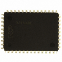
Manufacturer Part Number
ISP1760BEUM
Description
IC USB HOST CONTROLLER 128-LQFP
Manufacturer
ST-Ericsson Inc
Datasheet
1.ISP1760BEUM.pdf
(12 pages)
Specifications of ISP1760BEUM
Controller Type
USB Peripheral Controller
Interface
EHCI Interface
Voltage - Supply
3 V ~ 3.6 V
Operating Temperature
-40°C ~ 85°C
Mounting Type
Surface Mount
Package / Case
128-LQFP
Lead Free Status / RoHS Status
Lead free / RoHS Compliant
Current - Supply
-
Other names
568-1887-2
ISP1760BE,518
ISP1760BE-T
ISP1760BE,518
ISP1760BE-T
Available stocks
Company
Part Number
Manufacturer
Quantity
Price
Company:

Part Number:
ISP1760BEUM
Manufacturer:
JST
Quantity:
1 200
Part Number:
ISP1760BEUM
Manufacturer:
ST-ERICSSON
Quantity:
20 000


6
World News | May - June 2004 | Technology
Collaboration drives advanced process development
Unique collaboration speeds industrialization
Philips and IMEC strengthen link
New European project pushes the limits of CMOS technology
For leading consumer electronics companies, access to state-of-the-art
semiconductor technology is the key to delivering ever-richer consumer
experiences in areas such as multimedia entertainment and
communications. Philips is heavily involved in many cooperative projects
to ensure that new processes are available in plenty of time to meet
the demands of future applications.
Semiconductor manufacturers require advanced baseline CMOS technologies for the
powerful digital ICs at the heart of these applications. With 0.18 µm CMOS processes
widely used in today’s products, the drive towards future nodes on the CMOS roadmap
In conjunction with its Crolles2 Alliance partners – Motorola and STMicroelectronics – Philips
is advancing the next three CMOS baselines towards industrialization.The joint development
of these processes will keep the Alliance members ahead of the industry’s roadmap, and allow
their customers to exploit the performance, power, size and cost benefits earlier.
The most mature of these technologies is the 0.12 µm CMOS12, in which several devices
have already been produced, with many more in the pipeline. CMOS12 is a 1.2 V technology
with options optimized for high speed or low power. Embedded ROM, SRAM and DRAM
modules have been developed for CMOS12, and numerous IP blocks are available. These
include MIPS, ARM7 and ARM9 cores, TriMedia processors and USB functions as well as
general-purpose and I/O cells. A complete CMOS12 design environment has already been
released and support services are available.
Product development is also under way for CMOS090. The first tape-outs of this 90 nm
process were achieved in December 2003, and the first product was successfully processed
Royal Philips Electronics has signed a new agreement with the Inter-university MicroElectronics
Center (IMEC), one of the world’s leading independent research centers in nanoelectronics.
Following last year’s announcement of Philips’ participation as a Core Partner in IMEC’s
sub-45 nm research programs, the new deal extends Philips’ access to the advanced facilities
and expertise available within IMEC until the end of 2008. It will enable joint research
activities into advanced CMOS technologies in preparation of continued development and
commercialization within the Crolles2 Alliance, as well as joint development of more-
specialized semiconductor processes.
“Our previous collaboration with IMEC made possible important differentiators such as
our world-beating RF BiCMOS processes, highly effective non-volatile embedded memory
Seed-funded by the European Commission, the NanoCMOS project brings together some
of Europe’s leading research institutes and semiconductor companies.The project aims
to carry out the pioneering research into materials, processes, device architectures and
interconnections that is required to continue the drive towards increased semiconductor
performance and density.
The project’s first goal is to demonstrate the feasibility of 45 nm CMOS technology, which
it aims to do by 2005. At the same time, research into the next nodes on the international
technology roadmap (32 and 22 nm CMOS) will begin. This first phase is expected to last
27 months and mobilizes a large research potential. In addition to the € 24 million support
from the European Commission, the partners will invest advanced research resources to
achieve the project’s objectives.
Beginning in 2006, a proposed second phase will demonstrate the feasibility of the 32
and 22 nm nodes. Additionally, the consortium will make a proposal to the MEDEA+
organization to start in 2006. The proposal will cover the integration and validation of
is well under way. The Crolles2 Alliance is commercializing 120 and 90 nm processes,
and is already developing tomorrow’s 65 nm technology. Meanwhile, long-term research
collaborations are investigating the 45 nm node and beyond.
To complement CMOS technology, manufacturers also need special semiconductor processes
to produce chips that can handle associated tasks such as wireless communication, power
amplification and display driving. Again, Philips is active in joint research projects to drive
these advances. Its commitment to providing total system solutions rather than component
parts means that development of these specialized processes is as important to the company
as having cutting-edge CMOS.
earlier this year. A 1.0 / 1.2 V technology, CMOS090 will be available in general-purpose
and low-power versions. As well as ROM, SRAM and DRAM, a number of embedded
non-volatile memory options will be available. These include the familiar Flash memory
and EEPROM, but also new magnetoresistive RAM (MRAM) that combines the benefits
of SRAM, DRAM and Flash into a single memory type. A high-performance RF version of
CMOS090 is due to begin prototyping later this year.
Looking further into the future, development of the 65 nm CMOS065 process is
progressing rapidly at the Crolles2 facility. CMOS065 will be an evolution of CMOS090
and will be based on known technology modules. Due to be released during 2005,
CMOS065 will be available in general-purpose and low-power versions operating at
0.9 V and 1.2 V respectively. It will deliver logic densities twice as high as CMOS090
(four times those of CMOS12) and offer performance increases without additional leakage.
Many of the same options as for CMOS090 will eventually be available including Flash,
MRAM and RF.
solutions and best-in-class TrenchMOS devices,” said Theo Claasen, Executive Vice President
Technology and Strategy, Philips Semiconductors. “This new agreement with IMEC therefore
represents an important part of our strategy to keep Philips at the forefront of the
semiconductor industry.”
The agreement will run for five years and replaces an existing contract that was scheduled
to finish by mid 2005. It guarantees Philips a unique level of interaction with the expertise
of IMEC’s research scientists. Philips will also have access to the state-of-the-art equipment
within IMEC’s existing and newly built clean-room facilities.This will enable the development
of process steps for both 200 mm and 300 mm wafers, providing high-quality input to
Philips’ advanced production fabs.
the 45 nm node in an industrial 300 mm wafer manufacturing facility, currently expected to
be the Crolles2 facility. These two upcoming project proposals have been integrated into
the NanoCMOS strategy and discussed with European Commission and MEDEA+ officials.
“NanoCMOS has ambitious objectives and impressive resources mobilized towards a
common goal,” said Guillermo Bomchil, leader of the NanoCMOS project. “It represents
a unique opportunity for Europe to become the leading center for nanoelectronics, while
supporting academic research and helping its indigenous industrial players to hone their
competitive edge.”
The project involves Europe’s three largest semiconductor companies – Philips, Infineon
and STMicroelectronics – as well as the two biggest technical research institutes – CEA
Leti in France and IMEC in Belgium. Other partners include the Technical University of
Chemnitz (Germany), Ion Beam Services (France), ISILTEC (Germany), Magwel (Belgium),
ACIES Europe (France), the Fraunhofer-Gesellschaft (FhG) in Germany and the Centre
National de la Recherche Scientifique (CNRS) in France.
Technology continue
S e m i c o n d u c t o r s
cover
back
to
Related parts for ISP1760BEUM
Image
Part Number
Description
Manufacturer
Datasheet
Request
R

Part Number:
Description:
IC FILTR/CODEC 14BIT AUD 30TSSOP
Manufacturer:
ST-Ericsson Inc
Datasheet:
Part Number:
Description:
IC FILTR/CODEC 14BIT AUD 30TSSOP
Manufacturer:
ST-Ericsson Inc
Datasheet:

Part Number:
Description:
IC USB HUB CONTROLLER HS 80-LQFP
Manufacturer:
ST-Ericsson Inc
Datasheet:

Part Number:
Description:
IC USB OTG CONTROLLER 64-LQFP
Manufacturer:
ST-Ericsson Inc
Datasheet:

Part Number:
Description:
IC USB PERIPH CONTROLLER 64HVQFN
Manufacturer:
ST-Ericsson Inc
Datasheet:
Part Number:
Description:
IC USB HOST CTRL FULL-SPD 48HVQF
Manufacturer:
ST-Ericsson Inc
Datasheet:
Part Number:
Description:
IC USB CTRL HI-SPEED 64HVQFN
Manufacturer:
ST-Ericsson Inc
Datasheet:
Part Number:
Description:
IC USB CTRL HI-SPEED 64TFBGA
Manufacturer:
ST-Ericsson Inc
Datasheet:
Part Number:
Description:
IC USB CTRL HI-SPEED 64HVQFN
Manufacturer:
ST-Ericsson Inc
Datasheet:
Part Number:
Description:
IC USB CTRL SNGL CHIP 64TFBGA
Manufacturer:
ST-Ericsson Inc
Datasheet:
Part Number:
Description:
IC USB HOST/DEVICE CTRLR 64-LQFP
Manufacturer:
ST-Ericsson Inc
Datasheet:
Part Number:
Description:
IC USB CTRL HI-SPEED 128TFBGA
Manufacturer:
ST-Ericsson Inc
Datasheet:
Part Number:
Description:
IC USB CNTRLR FULL-SPD 48-TSSOP
Manufacturer:
ST-Ericsson Inc
Datasheet: