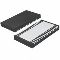
LTC4269CDKD-2#PBF Linear Technology, LTC4269CDKD-2#PBF Datasheet - Page 5

LTC4269CDKD-2#PBF
Manufacturer Part Number
LTC4269CDKD-2#PBF
Description
IC PD/SYNC FORWARD CTRLR 32-DFN
Manufacturer
Linear Technology
Type
Power Over Ethernet (PoE)r
Datasheet
1.LTC4269CDKD-2PBF.pdf
(34 pages)
Specifications of LTC4269CDKD-2#PBF
Applications
Power Interface Switch for Power Over Ethernet (PoE) Devices
Voltage - Supply
14 V ~ 16 V
Operating Temperature
0°C ~ 70°C
Mounting Type
Surface Mount
Package / Case
32-DFN
Current - Supply
1.35mA
Interface
IEEE 802.3af
Controller Type
Powered Device Interface Controller (PD)
Lead Free Status / RoHS Status
Lead free / RoHS Compliant
Available stocks
Company
Part Number
Manufacturer
Quantity
Price
elecTrical characTerisTics
PARAMETER
SOUT High Level
SOUT Active Pull-Off in Shutdown
SOUT to OUT (Rise) DELAY (t
V
OUT Driver
OUT Rise Time
OUT Fall Time
OUT Clamp Voltage
OUT Low Level
OUT High Level
OUT Active Pull-Off in Shutdown
OUT Max Duty Cycle
OUT Max Duty Cycle Clamp
Soft-Start
SS_MAXDC Low Level: V
SS_MAXDC Soft-Start Reset Threshold
SS_MAXDC Active Threshold
SS_MAXDC Input Current
(Soft-Start Pull-Down: I
Note 1: Stresses beyond those listed under Absolute Maximum Ratings
may cause permanent damage to the device. Exposure to any Absolute
Maximum Rating condition for extended periods may affect device
reliability and lifetime.
Note 2: Pins with 100V absolute maximum guaranteed for T ≥ 0°C,
otherwise 90V.
Note 3: PWRGD voltage clamps at 14V with respect to V
Note 4: In applications where the V
network from a system V
V
Note 5: All voltages are with respect to V
Note 6: Input voltage specifications are defined with respect to LTC4269-2
pins and meet IEEE 802.3af/at specifications when the input diode bridge
is included.
Note 7: Signature resistance is measured via the ∆V/∆I method with the
minimum ∆V of 1V. The LTC4269-2 signature resistance accounts for the
additional series resistance in the input diode bridge.
temperature range, otherwise specifications are at T
DELAY
IN ON(MAX)
< V
Z
< 25V should be connected from the V
DIS
IN
OL
)
> 25V, an external Zener with clamp voltage
DELAY
)
IN
pin is supplied via an external RC
PORTN
pin unless otherwise noted.
CONDITIONS
I
V
COMP = 2.5V, FB = 1V (Note 16)
R
FB = 1V, C
FB = 1V, C
I
I
I
I
I
V
COMP = 2.5V, FB = 1V, R
V
COMP = 2.5V, FB = 1V, R
V
I
Measured on SS_MAXDC
FB + 1V, DC > 0%
SS_MAXDC = 1V, SD_V
IN
GATE
GATE
GATE
GATE
GATE
GATE
SS_MAXDC
NEG
IN
DELAY
IN
IN
IN
SD_V
SD_V
pin to GND.
= 10V, SD_V
= 5V, SD_V
= 5V, SD_V
= 10V
.
A
= –25mA, V
= 0µA, COMP = 2.5V, FB = 1V
= 20mA
= 200mA
= –20mA, V
= –200mA, V
= 25°C.
= 120k
SEC
SEC
L
L
= 150µA, OC = 1V
= 1.32V, SS_MAXDC = 1.84V
= 2.64V, SS_MAXDC = 1.84V
= 1nF (Notes 15, 16)
= 1nF (Notes 15, 16)
The
SEC
SEC
SEC
IN
IN
l
= 0V, SOUT = 1V
IN
= 0V, OUT = 1V
= 12V COMP = 2.5V, FB = 1V
= 12V COMP = 2.5V, FB = 1V
= 1.4V, SS_MAXDC = V
denotes the specifications which apply over the full operating
= 12V COMP = 2.5V, FB = 1V
SEC
DELAY
DELAY
Note 8: An invalid signature after the 1st classification event is mandated
by IEEE 802.3at standard. See the Applications Information section.
Note 9: Class accuracy is respect to the ideal current defined as
1.237/R
Note 10: This parameter is assured by design and wafer level testing.
Note 11: Voltages are with respect to GND unless otherwise specified.
Tested with COMP open, V
set to V
= 121k, R
SOUT open, unless otherwise specified.
Note 12: Guaranteed by correlation to static test.
Note 13: V
scaled by × 1.18 (to correlate to worst-case V
Note 14: Maximum recommended SYNC frequency = 500kHz.
Note 15: Guaranteed but not tested.
Note 16: Timing for R = 40k derived from measurement with R = 240k.
= 1.4V, OC = 1V
= 10k (f
= 10k (f
REF
CLASS
DELAY
IN
(but electrically isolated), C
OSC
OSC
start-up current is measured at V
and does not include variations in R
= 121k, V
= 200kHz),
= 200kHz),
REF
ISENSE
FB
= 1.4V, R
= 0V, V
11.5
9.75
63.5
MIN
9.9
10
20
83
25
ROSC
1
VREF
OC
= 0V, C
= 178k, V
= 0.1µF , V
IN
IN
LTC4269-2
0.45
1.25
0.45
TYP
120
800
0.9
0.2
0.8
40
50
30
13
90
72
33
start-up current at V
OUT
= V
CLASS
IN(ON)
= 1nF , V
SYNC
SD_VSEC
resistance.
MAX
14.5
0.75
80.5
1.8
= 0V, V
– 0.25V and
41
IN
= 2V, R
= 15V,
SS(MAXDC)
BLANK
IN(ON)
42692fb
UNITS
mA
mA
µA
ns
ns
ns
ns
%
%
%
V
V
V
V
V
V
V
V
V
V
.


