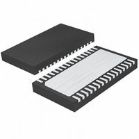
LTC4269CDKD-1#TRPBF Linear Technology, LTC4269CDKD-1#TRPBF Datasheet - Page 13

LTC4269CDKD-1#TRPBF
Manufacturer Part Number
LTC4269CDKD-1#TRPBF
Description
IC PD/OPTO FLYBACK CTRLR 32-DFN
Manufacturer
Linear Technology
Type
Power Over Ethernet (PoE)r
Datasheet
1.LTC4269IDKD-1PBF.pdf
(44 pages)
Specifications of LTC4269CDKD-1#TRPBF
Applications
Power Interface Switch for Power Over Ethernet (PoE) Devices
Voltage - Supply
14 V ~ 16 V
Operating Temperature
0°C ~ 70°C
Mounting Type
Surface Mount
Package / Case
32-DFN
Current - Supply
1.35mA
Interface
IEEE 802.3af
Controller Type
Powered Device Interface Controller (PD)
Lead Free Status / RoHS Status
Lead free / RoHS Compliant
Available stocks
Company
Part Number
Manufacturer
Quantity
Price
APPLICATIONS INFORMATION
Table 1. LTC4269-1 Modes of Operation as a Function
of Input Voltage
V
0V to 1.4V
1.5V to 9.8V
(5.4V to 9.8V)
12.5V to ON/OFF*
ON/OFF* to 60V
>71V
*ON/OFF includes hysteresis. Rising input threshold, 37.2V Max.
These modes satisfy the requirements defi ned in the
IEEE 802.3af/IEEE 802.3at specifi cation.
INPUT DIODE BRIDGE
In the IEEE 802.3af/IEEE 802.3at standard, the modes of
operation reference the input voltage at the PD’s RJ45
connector. Since the PD must handle power received in
either polarity from either the data or the spare pair, input
diode bridges BR1 and BR2 are connected between the
RJ45 connector and the LTC4269-1 (Figure 2).
PORTP
Falling input threshold, 30V Min.
–V
PORTN
(V)
LTC4269-1 MODES OF OPERATION
Inactive (Reset After 1st Classifi cation Event)
25k Signature Resistor Detection Before 1st
Classifi cation Event (Mark, 11k Signature
Corrupt After 1st Classifi cation Event)
Classifi cation Load Current Active
Inrush and Power Applied To PD Load
Overvoltage Lockout,
Classifi cation and Hot Swap Are Disabled
Figure 2. PD Front End Using Diode Bridges on Main and Spare Inputs
POWERED
DEVICE
INPUT
(PD)
RJ45
1
2
3
6
4
5
7
8
TX
TX
RX
RX
SPARE
SPARE
+
–
+
–
+
–
T1
BR2
TO PHY
The input diode bridge introduces a voltage drop that
affects the range for each mode of operation. The
LTC4269-1 compensates for these voltage drops so that a
PD built with the LTC4269-1 meets the IEEE 802.3af/IEEE
802.3at-established voltage ranges. Note the Electrical
Characteristics are referenced with respect to the
LTC4269- 1 package pins.
DETECTION
During detection, the PSE looks for a 25k signature resis-
tor which identifi es the device as a PD. The PSE will apply
two voltages in the range of 2.8V to 10V and measures
the corresponding currents. Figure 1 shows the detection
voltages V1 and V2 and the corresponding PD current. The
PSE calculates the signature resistance using the ΔV/ΔI
measurement technique.
The LTC4269-1 presents its precision, temperature-com-
pensated 25k resistor between the V
pins, alerting the PSE that a PD is present and requests
power to be applied. The LTC4269-1 signature resistor
also compensates for the additional series resistance
introduced by the input diode bridge. Thus a PD built
with the LTC4269-1 conforms to the IEEE 802.3af/IEEE
802.3at specifi cations.
0.1μF
100V
BR1
D3
V
LTC4269-1
PORTN
V
PORTP
42691 F02
LTC4269-1
PORTP
and V
13
PORTN
42691fb


