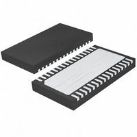
LTC4269CDKD-2#TRPBF Linear Technology, LTC4269CDKD-2#TRPBF Datasheet - Page 25

LTC4269CDKD-2#TRPBF
Manufacturer Part Number
LTC4269CDKD-2#TRPBF
Description
IC PD/SYNC FORWARD CTRLR 32-DFN
Manufacturer
Linear Technology
Type
Power Over Ethernet (PoE)r
Datasheet
1.LTC4269CDKD-2PBF.pdf
(34 pages)
Specifications of LTC4269CDKD-2#TRPBF
Applications
Power Interface Switch for Power Over Ethernet (PoE) Devices
Voltage - Supply
14 V ~ 16 V
Operating Temperature
0°C ~ 70°C
Mounting Type
Surface Mount
Package / Case
32-DFN
Current - Supply
1.35mA
Interface
IEEE 802.3af
Controller Type
Powered Device Interface Controller (PD)
Lead Free Status / RoHS Status
Lead free / RoHS Compliant
Available stocks
Company
Part Number
Manufacturer
Quantity
Price
Part Number:
LTC4269CDKD-2#TRPBFLTC4269CDKD-2#PBF
Manufacturer:
Linear Technology
Quantity:
135
applicaTions inForMaTion
where:
Programming Slope Compensation
The LTC4269-2 uses a current mode architecture to provide
fast response to load transients and to ease frequency
compensation requirements. Current mode switching
regulators which operate with duty cycles above 50%
and have continuous inductor current must add slope
compensation to their current sensing loop to prevent
subharmonic oscillations. (For more information on slope
compensation, see Application Note 19.) The LTC4269-2
has programmable slope compensation to allow a wide
range of inductor values, to reduce susceptibility to PCB
generated noise and to optimize loop bandwidth. The
LTC4269-2 programs slope compensation by inserting a
resistor, R
The LTC4269-2 generates a current at the I
is linear from 0% duty cycle to the maximum duty cycle
of the OUT pin. A simple calculation of I
gives an added ramp to the voltage at the I
programmable slope compensation. (See both graphs
I
Threshold vs Duty Cycle in the Typical Performance
Characteristics section.)
SENSE
R
I
N
N
LTC4269-2
RIPPLE
CURRENT SLOPE = 35µA • DC
S
S
P
= sense resistor in source of primary MOSFET
= number of transformer secondary turns
= number of transformer primary turns
I
SENSE
Pin Current vs Duty Cycle and I
OUT
OC
Figure 13. Programming Slope Compensation
SLOPE
= I
P-P
R
SLOPE
, in series with the I
ripple current in the output inductor L1
V
R
42692 F13
SOURCE
S
V
I
DC = DUTY CYCLE
FOR SYNC OPERATION
I
k = f
SENSE
SENSE(SYNC)
(ISENSE)
OSC
= 8µA + 35DC µA
/f
SENSE
SYNC
= V
SOURCE
= 8µA + (k • 35DC)µA
SENSE
pin (Figure 13).
SENSE
SENSE
+ (I
SENSE
SENSE
Maximum
pin which
• R
• R
pin for
SLOPE
SLOPE
)
Programming Synchronous Rectifier Timing:
SOUT to OUT delay (‘t
The LTC4269-2 has an additional output SOUT which pro-
vides a ±50mA peak drive clamped to 12V. In applications
requiring synchronous rectification for high efficiency,
the LTC4269-2 SOUT provides a sync signal for second-
ary side control of the synchronous rectifier MOSFETs
(Figure 14). Timing delays through the converter can
cause non-optimum control timing for the synchronous
rectifier MOSFETs. The LTC4269-2 provides a program-
mable delay (t
edge and OUT rising edge to optimize timing control for
the synchronous rectifier MOSFETs to achieve maximum
efficiency gains. A resistor R
DELAY pin to GND sets the value of t
for t
with R
Characteristics section).
Programming Maximum Duty Cycle Clamp
For forward converter applications, a maximum switch
duty cycle clamp which adapts to transformer input volt-
age is necessary for reliable control of the MOSFETs. This
volt-second clamp provides a safeguard for transformer
reset that prevents transformer saturation. The LTC4269-2
SD_V
programmable volt-second clamp solution using simple
resistor ratios (Figure 15).
An increase of voltage at the SD_V
maximum duty cycle clamp to decrease. Deriving SD_V
from a resistor divider connected to system input voltage
DELAY
Figure 14. Programming SOUT and OUT Delay: t
SEC
DELAY
SOUT
OUT
and SS_MAXDC pins provide a capacitor-less,
range from 10ns with R
= 160k (see graph in the Typical Performance
DELAY
t
DELAY
, Figure 14) between SOUT rising
DELAY
’)
LTC4269-2
DELAY
DELAY
42692 F14
DELAY
LTC4269-2
DELAY
connected from the
SEC
= 10k to 160ns
pin causes the
. Typical values
R
DELAY
DELAY
42692fb
SEC


