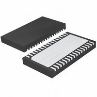
LTC4269IDKD-1#TRPBF Linear Technology, LTC4269IDKD-1#TRPBF Datasheet - Page 32

LTC4269IDKD-1#TRPBF
Manufacturer Part Number
LTC4269IDKD-1#TRPBF
Description
IC PD/OPTO FLYBACK CTRLR 32-DFN
Manufacturer
Linear Technology
Type
Power Over Ethernet (PoE)r
Datasheet
1.LTC4269IDKD-1PBF.pdf
(44 pages)
Specifications of LTC4269IDKD-1#TRPBF
Applications
Power Interface Switch for Power Over Ethernet (PoE) Devices
Voltage - Supply
14 V ~ 16 V
Operating Temperature
-40°C ~ 85°C
Mounting Type
Surface Mount
Package / Case
32-DFN
Current - Supply
1.35mA
Interface
IEEE 802.3af
Controller Type
Powered Device Interface Controller (PD)
Lead Free Status / RoHS Status
Lead free / RoHS Compliant
Available stocks
Company
Part Number
Manufacturer
Quantity
Price
APPLICATIONS INFORMATION
LTC4269-1
The LTC4269-1 has an internal clamp on V
mately 19.5V. This provides some protection for the part
in the event that the switcher is off (UVLO low) and the
V
should never attain this clamp voltage.
Control Loop Compensation
Loop frequency compensation is performed by connect-
ing a capacitor network from the output of the feedback
amplifi er (V
Because of the sampling behavior of the feedback amplifi er,
compensation is different from traditional current mode
controllers. Normally only C
be used to add a zero, but the phase margin improvement
traditionally offered by this extra resistor is usually already
accomplished by the nonzero secondary circuit impedance.
C
pole and is usually sized at 0.1 times C
In further contrast to traditional current mode switchers,
V
The dynamic nature of the clamped feedback amplifi er
forms an effective track/hold type response, whereby the
V
held during the subsequent switch-on portion of the next
cycle. This action naturally holds the V
during the current comparator sense action (current mode
switching).
Application Note 19 provides a method for empirically
tweaking frequency compensation. Basically, it involves
introducing a load current step and monitoring the
response.
32
CMP
CC
VCMP2
CMP
node is pulled high. If R
pin ripple is generally not an issue with the LTC4269-1.
voltage changes during the fl yback pulse, but is then
can be used to add an additional high frequency
Figure 15. V
CMP
pin) to ground as shown in Figure 15.
V
CMP
17
CMP
Compensation Network
42691 F15
C
VCMP2
TR
VCMP
is sized correctly, the part
is required. R
R
VCMP
C
VCMP
CMP
VCMP
CC
voltage stable
.
of approxi-
VCMP
can
Slope Compensation
The LTC4269-1 incorporates current slope compensation.
Slope compensation is required to ensure current loop
stability when the DC is greater than 50%. In some switching
regulators, slope compensation reduces the maximum peak
current at higher duty cycles. The LTC4269-1 eliminates
this problem by having circuitry that compensates for
the slope compensation so that maximum current sense
voltage is constant across all duty cycles.
Minimum Load Considerations
At light loads, the LTC4269-1 derived regulator goes into
forced continuous conduction mode. The primary-side
switch always turns on for a short time as set by the
t
load requires, power will fl ow back into the primary dur-
ing the off period when the synchronization switch is on.
This does not produce any inherently adverse problems,
although light load effi ciency is reduced.
Maximum Load Considerations
The current mode control uses the V
and amplifi ed sense resistor voltage as inputs to the
current comparator. When the amplifi ed sense voltage
exceeds the V
is turned off.
In normal use, the peak switch current increases while
FB is below the internal reference. This continues until
V
MOSFET will turn off at the rated 100mV V
repeats on the next cycle.
It is possible for the peak primary switch currents as
referred across R
because of the minimum switch on time blanking. If the
voltage on V
turn-on time, the SFST capacitor is discharged, causing
the discharge of the V
the peak current on the next cycle and will reduce overall
stress in the primary switch.
ON(MIN)
CMP
reaches its 2.56V clamp. At clamp, the primary-side
resistor. If this produces more power than the
SENSE
CMP
SENSE
node voltage, the primary-side switch
exceeds 205mV after the minimum
CMP
to exceed the max 100mV rating
capacitor. This then reduces
CMP
SENSE
node voltage
level. This
42691fb


