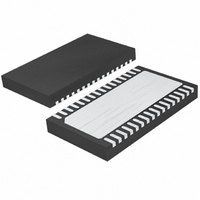
LTC4269IDKD-2#PBF Linear Technology, LTC4269IDKD-2#PBF Datasheet - Page 26

LTC4269IDKD-2#PBF
Manufacturer Part Number
LTC4269IDKD-2#PBF
Description
IC PD/SYNC FORWARD CTRLR 32-DFN
Manufacturer
Linear Technology
Type
Power Over Ethernet (PoE)r
Datasheet
1.LTC4269CDKD-2PBF.pdf
(34 pages)
Specifications of LTC4269IDKD-2#PBF
Applications
Power Interface Switch for Power Over Ethernet (PoE) Devices
Voltage - Supply
14 V ~ 16 V
Operating Temperature
-40°C ~ 85°C
Mounting Type
Surface Mount
Package / Case
32-DFN
Current - Supply
1.35mA
Interface
IEEE 802.3af
Controller Type
Powered Device Interface Controller (PD)
Operating Temperature (max)
85C
Operating Temperature (min)
-40C
Pin Count
32
Mounting
Surface Mount
Package Type
DFN EP
Case Length
7mm
Screening Level
Industrial
Lead Free Status / RoHS Status
Lead free / RoHS Compliant
Available stocks
Company
Part Number
Manufacturer
Quantity
Price
LTC4269-2
applicaTions inForMaTion
creates the volt-second clamp. The maximum duty cycle
clamp can be adjusted by programming voltage on the
SS_MAXDC pin using a resistor divider from V
increase of voltage at the SS_MAXDC pin causes the
maximum duty cycle clamp to increase.
To program the volt-second clamp, the following steps
should be taken:
(1) The maximum operational duty cycle of the converter
(2) An initial value for the maximum duty cycle clamp
Note: Since maximum operational duty cycle occurs at
minimum system input voltage (UVLO), the voltage at the
SD_V
where:
Max Duty Cycle Clamp (OUT Pin) =
k • 0.522(SS_MAXDC(DC)/SD_V
SS_MAXDC(DC) = V
SD_V
t
k = 1.11 – 5.5e–7 • (f
DELAY
should be calculated for the given application.
should be calculated using the equation below with a
first pass guess for SS_MAXDC.
Figure 15. Programming Maximum Duty Cycle Clamp
SEC
CLAMP INPUT
SEC
DUTY CYCLE
= programmed delay between SOUT and OUT
pin = 1.32V.
ADAPTIVE
= 1.32V at minimum system input voltage
*MINIMUM ALLOWABLE R
GUARANTEE SOFT-START PULL-OFF
POWER SUPPLY
INPUT VOLTAGE
REF
OSC
R1
R2
(R
)
R
B
B
/(R
R
T
*
T
T
MAX DUTY CYCLE
CLAMP ADJUST INPUT
IS 10k TO
+ R
SD_V
SS_MAXDC
V
SEC
REF
LTC4269-2
B
SEC
) – (t
)
42692 F15
DELAY
REF
• f
OSC
. An
)
(3) The maximum duty cycle clamp calculated in (2)
Example calculation for (2):
Note 1: To achieve the same maximum duty cycle clamp at
100kHz as calculated for 200kHz, the SS_MAXDC voltage
should be reprogrammed by,
Note 2 : To achieve the same maximum duty cycle clamp
while synchronizing to an external clock at the SYNC pin,
the SS_MAXDC voltage should be reprogrammed as,
Programming Soft-Start Timing
The LTC4269-2 has built-in soft-start capability to provide
low stress controlled start-up from a list of fault condi-
tions that can occur in the application (see Figures 16
and 17). The LTC4269-2 provides true PWM soft-start by
For R
R
this gives SS_MAXDC(DC) = 1.84V, t
and k = 1
Maximum Duty Cycle Clamp
= 1 • 0.522(1.84/1.32) – (40ns • 200kHz)
= 0.728 – 0.008 = 0.72 (Duty Cycle Clamp = 72%)
SS_MAXDC(DC) (100kHz)
= SS_MAXDC(DC) (200kHz) • k (200kHz)/k (100kHz)
= 1.84 • 1.0/1.055 = 1.74V (k = 1.055 for 100kHz)
SS_MAXDC (DC) (fsync)
= SS_MAXDC (DC) (200kHz) • [(fosc/fsync) +
0.09(fosc/200kHz)0.6]
For SS_MAXDC (DC) (200kHz) = 1.84V for 72%
duty cycle
SS_MAXDC (DC) (fsync = 250kHz) for 72%
duty cycle
= 1.84 • [(200kHz/250kHz) + 0.09(1)0.6]
= 1.638V
should be programmed to be 10% greater than the
maximum operational duty cycle calculated in (1).
Simple adjustment of maximum duty cycle can be
achieved by adjusting SS_MAXDC.
DELAY
T
= 35.7k, R
= 40k, f
OSC
B
= 100k, V
= 200kHz and SD_V
REF
= 2.5V,
DELAY
SEC
= 40ns
= 1.32V,
42692fb


