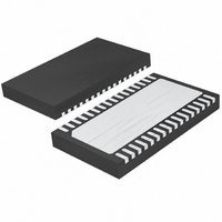
LTC4269IDKD-2#PBF Linear Technology, LTC4269IDKD-2#PBF Datasheet - Page 28

LTC4269IDKD-2#PBF
Manufacturer Part Number
LTC4269IDKD-2#PBF
Description
IC PD/SYNC FORWARD CTRLR 32-DFN
Manufacturer
Linear Technology
Type
Power Over Ethernet (PoE)r
Datasheet
1.LTC4269CDKD-2PBF.pdf
(34 pages)
Specifications of LTC4269IDKD-2#PBF
Applications
Power Interface Switch for Power Over Ethernet (PoE) Devices
Voltage - Supply
14 V ~ 16 V
Operating Temperature
-40°C ~ 85°C
Mounting Type
Surface Mount
Package / Case
32-DFN
Current - Supply
1.35mA
Interface
IEEE 802.3af
Controller Type
Powered Device Interface Controller (PD)
Operating Temperature (max)
85C
Operating Temperature (min)
-40C
Pin Count
32
Mounting
Surface Mount
Package Type
DFN EP
Case Length
7mm
Screening Level
Industrial
Lead Free Status / RoHS Status
Lead free / RoHS Compliant
Available stocks
Company
Part Number
Manufacturer
Quantity
Price
LTC4269-2
applicaTions inForMaTion
The time for SS_MAXDC to fall to a given voltage can be
approximated as:
where:
For faults arising from (1) and (2):
Example
If the OC fault is not removed before 185µs then SS_MAXDC
will continue to fall past 0.45V towards a new V
The typical V
SS_MAXDC Charge Timing
When all faults are removed and the SS_MAXDC pin
has fallen to its reset threshold of 0.45V or lower, the
SS_MAXDC pin will be released and allowed to charge.
SS_MAXDC will rise until it settles at its programmed DC
voltage—setting the maximum switch duty cycle clamp.
SS_MAXDC(t
(C
I
C
SS_MAXDC(DC) = programmed DC voltage
V
recharge
I
V
For a fault arising from (3):
V
SS_MAXDC(DC) = V
V
(if fault removed before t
For an overcurrent fault (OC > 100mV), V
R
V
I
= 8e
SS_MAXDC(DC) = 1.84V
SS_MAXDC(t
= (1e
DIS
DIS
DIS
SS
SS(MIN)
REF
REF
SS(MIN)
SS(MIN)
T
SS
= 35.7k, R
= net discharge current on C
= capacitor value at SS_MAXDC pin
≅ 8e
≅ 8e
–4
/I
–7
= 100mV.
= 2.5V.
DIS
+ (2.05)(–0.23e
/7.5e
–4
–4
) • [SS_MAXDC(DC) – V
= minimum SS_MAXDC voltage before
= SS_MAXDC reset threshold = 0.45V
= 0.45V,
OL
+ (V
+ (2.5 – 0.45)[(½ • 100k) – (1/35.7k)]
–4
for SS_MAXDC at 150µA is 0.2V.
FALL
B
FALL
) • (1.84 – 0.45)=1.85e
= 100k, C
REF
)=
)
– V
REF
SS(MIN)
–4
[R
SS
FALL
) = 7.5e
B
/(R
= 0.1µF and assume
)
)[(1/2R
T
+ R
–4
SS
SS(MIN)
B
)]
B
–4
) – (1/R
s
]
REF
= 2.5V,
T
SS(MIN)
)]
.
The calculation of charging time for the SS_MAXDC pin
between any two voltage levels can be approximated as
an RC charging waveform using the model shown in
Figure 16.
The ability to predict SS_MAXDC rise time between any two
voltages allows prediction of several key timing periods:
The time for SS_MAXDC to charge to a given voltage V
is found by re-arranging:
to give,
where,
Example (1) No Switching Period
The period of no switching for the converter, when a soft-
start event has occurred, depends on how far SS_MAXDC
can fall before recharging occurs and how long a fault ex-
ists. It will be assumed that a fault triggering soft-start is
removed before SS_MAXDC can reach its reset threshold
(0.45V).
t
(1) No Switching Period (time from SS_MAXDC(DC) to
(2) Converter Output Rise Time (time from V
(3) Time For Maximum Duty Cycle Clamp within X% of
DISCHARGE
V
t = RC • (–1) • ln(1 – V
V
SS_MAXDC(DC) = programmed DC voltage setting
maximum duty cycle clamp = V
R = R
C = C
No Switching Period = t
t
0.45V
t
DISCHARGE
CHARGE
V
V
maximum duty cycle clamp equals the natural duty
cycle of the switch)
Target Value
SS
SS
SS(MIN)
SS(REG)
(t) = SS_MAXDC(DC) (1 – e
= SS_MAXDC voltage at time t
SS
CHARGE
(Figure 16)
= charge time from 0.45V to V
was already calculated earlier as 185µs.
; V
+ time from V
= discharge time from SS_MAXDC(DC) to
SS(REG)
(Figure 16) = R
is the level of SS_MAXDC where
SS
DISCHARGE
SS(MIN)
/SS_MAXDC(DC))
T
• R
REF
(–t/RC)
to V
B
/(R
+ t
(R
SS(ACTIVE)
B
CHARGE
T
)
/(R
SS(ACTIVE)
+ R
T
SS(ACTIVE
B
+ R
)
)
B
)
42692fb
) to
SS


