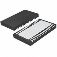
LTC4269IDKD-2#TRPBF Linear Technology, LTC4269IDKD-2#TRPBF Datasheet - Page 21

LTC4269IDKD-2#TRPBF
Manufacturer Part Number
LTC4269IDKD-2#TRPBF
Description
IC PD/SYNC FORWARD CTRLR 32-DFN
Manufacturer
Linear Technology
Type
Power Over Ethernet (PoE)r
Datasheet
1.LTC4269CDKD-2PBF.pdf
(34 pages)
Specifications of LTC4269IDKD-2#TRPBF
Applications
Power Interface Switch for Power Over Ethernet (PoE) Devices
Voltage - Supply
14 V ~ 16 V
Operating Temperature
-40°C ~ 85°C
Mounting Type
Surface Mount
Package / Case
32-DFN
Current - Supply
1.35mA
Interface
IEEE 802.3af
Controller Type
Powered Device Interface Controller (PD)
Lead Free Status / RoHS Status
Lead free / RoHS Compliant
Available stocks
Company
Part Number
Manufacturer
Quantity
Price
applicaTions inForMaTion
An additional output signal is included for synchronous
rectifier control or active clamp control. A precision 107mV
threshold senses overcurrent conditions and triggers soft-
start for low stress short-circuit protection and control.
The key functions of the LTC4269-2 PWM controller are
shown in the Block Diagrams.
Part Start-Up
In normal operation, the SD_V
and the V
to turn on. This combination of pin voltages allows the
2.5V V
control circuitry and providing up to 2.5mA external drive.
SD_V
the power supply undervoltage lockout (UVLO) threshold
on the input voltage to the forward converter. Hysteresis
on the UVLO threshold can also be programmed since
the SD_V
0µA after part turn-on.
With the LTC4269-2 turned on, the V
low as 8.75V before part shutdown occurs. This V
hysteresis (5.5V) combined with low 460µA start-up input
current allows low power start-up using a resistor/capaci-
tor network from power supply input voltage to supply
the V
to prevent V
a bias winding in the converter takes over supply to the
V
Output Drivers
The LTC4269-2 has two outputs, SOUT and OUT. The OUT
pin provides a ±1A peak MOSFET gate drive clamped to
13V. The SOUT pin has a ±50mA peak drive clamped to
12V and provides sync signal timing for synchronous
rectification control or active clamp control.
For SOUT and OUT turn-on, a PWM latch is set at the
start of each main oscillator cycle. OUT turn-on is delayed
from SOUT turn-on by a time, t
is programmed using a resistor from the DELAY pin to
GND and is used to set the timing control of the secondary
synchronous rectifiers for optimum efficiency.
SOUT and OUT turn off at the same time each cycle by
one of three methods:
IN
pin.
IN
SEC
REF
pin (Figure 10). The V
threshold can be used for externally programming
SEC
IN
pin to become active, supplying the LTC4269-2
IN
pin must exceed 14.25V to allow the part
pin draws 11µA just before part turn-on and
falling below its turn-off threshold before
IN
SEC
capacitor value is chosen
DELAY
pin must exceed 1.32V
IN
(Figure 14). t
pin can drop as
IN
DELAY
pin
During any of the following conditions—low V
SD_V
start event is latched and both SOUT and OUT turn off
immediately (Figure 11).
Leading Edge Blanking
To prevent MOSFET switching noise causing premature
turn-off of SOUT or OUT, programmable leading edge
blanking exists. This means both the current sense com-
parator and overcurrent comparator outputs are ignored
during MOSFET turn-on and for an extended period after
the OUT leading edge (Figure 12). The extended blanking
period is programmable by adjusting a resistor from the
BLANK pin to GND.
Adaptive Maximum Duty Cycle Clamp
(Volt-Second Clamp)
For forward converter applications, a maximum switch
duty cycle clamp which adapts to transformer input volt-
age is necessary for reliable control of the MOSFET. This
volt-second clamp provides a safeguard for transformer
reset that prevents transformer saturation. Instantaneous
load changes can cause the converter loop to demand
maximum duty cycle. If the maximum duty cycle of the
switch is too great, the transformer reset voltage can ex-
ceed the voltage rating of the primary-side MOSFETs with
catastrophic damage. Many converters solve this problem
by limiting the operational duty cycle of the MOSFET to
50% or less—or by using a fixed (non-adaptive) maximum
duty cycle clamp with very large voltage rated MOSFETs.
The LTC4269-2 provides a volt-second clamp to allow
MOSFET duty cycles well above 50%. This gives greater
power utilization for the MOSFETs, rectifiers and trans-
former resulting in less space for a given power output.
In addition, the volt-second clamp can allow a reduced
voltage rating on the MOSFET resulting in lower R
for greater efficiency. The volt-second clamp defines a
maximum duty cycle ‘guard rail’ which falls when power
supply input voltage increases.
(1) MOSFET peak current sense at I
(2) Adaptive maximum duty cycle clamp reached during
(3) Maximum duty cycle reset of the PWM latch
load/line transients
SEC
or overcurrent detection at the OC pin—a soft-
LTC4269-2
SENSE
pin
IN
DS(ON)
, low
42692fb


