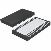
LTC4269IDKD-2#TRPBF Linear Technology, LTC4269IDKD-2#TRPBF Datasheet - Page 29

LTC4269IDKD-2#TRPBF
Manufacturer Part Number
LTC4269IDKD-2#TRPBF
Description
IC PD/SYNC FORWARD CTRLR 32-DFN
Manufacturer
Linear Technology
Type
Power Over Ethernet (PoE)r
Datasheet
1.LTC4269CDKD-2PBF.pdf
(34 pages)
Specifications of LTC4269IDKD-2#TRPBF
Applications
Power Interface Switch for Power Over Ethernet (PoE) Devices
Voltage - Supply
14 V ~ 16 V
Operating Temperature
-40°C ~ 85°C
Mounting Type
Surface Mount
Package / Case
32-DFN
Current - Supply
1.35mA
Interface
IEEE 802.3af
Controller Type
Powered Device Interface Controller (PD)
Lead Free Status / RoHS Status
Lead free / RoHS Compliant
Available stocks
Company
Part Number
Manufacturer
Quantity
Price
applicaTions inForMaTion
t
Step 1:
Step 2:
t(V
Step 3:
t(V
From Step 1 and Step 2
The total time of no switching for the converter due to a
soft-start event
Example (2) Converter Output Rise Time
The rise time for the converter output to reach regulation
can be closely approximated as the time between the start
of switching (SS_MAXDC = V
converter duty cycle is in regulation (DC(REG)) and no
longer controlled by SS_MAXDC (SS_MAXDC = V
Converter output rise time can be expressed as:
Step 1: Determine converter duty cycle DC(REG) for output
in regulation.
The natural duty cycle DC(REG) of the converter depends
on several factors. For this example it is assumed that
DC(REG) = 60% for power supply input voltage near the
power supply UVLO. This gives SD_V
CHARGE
V
V
t
SS_MAXDC(DC) = 2.5[100k/(35.7k + 100k)] = 1.84V
R
t = R
= 2.63e
= 2.63e
t = R
= 2.63e
= 2.63e
t
= t
Output Rise Time = t(V
SS
SS
CHARGE
CHARGE
REF
SS(MIN)
CHARGE
DISCHARGE
= 0.45V) is calculated from:
= 0.8V) is calculated from:
CHARGE
CHARGE
= 2.5V, R
is calculated by assuming the following:
4
–3
4
–3
= t(V
= (1.5 – 0.73)e
= 0.45V.
• 1e
• 1e
= (35.7k • 100k/135.7k) = 26.3k
• (–1) • ln(0.755) = 7.3e
• (–1) • ln(0.565) = 1.5e
• C
• C
–7
–7
+ t
SS
T
SS
SS
CHARGE
• (–1) • ln(1 – 0.45/1.84)
• (–1) • ln(1 – 0.8/1.84)
= 0.8V) – t(V
= 35.7k, R
• (–1) • ln(1 – V
• (–1) • ln(1 – V
SS(REG)
= 1.85e
–3
SS(ACTIVE)
s = 7.7e
B
= 100k, C
SS
) – t(V
–4
= 0.45V)
SS
+ 7.7e
SS
–4
–4
–3
) and the time where
SEC
/SS_MAXDC(DC))
/SS–MAXDC(DC))
SS(ACTIVE)
s
s
s
SS
= 1.32V.
–4
= 0.1µF and
= 9.55e
SS(REG)
)
–4
s
).
Also assume that the maximum duty cycle clamp pro-
grammed for this condition is 72% for SS_MAXDC(DC)
= 1.84V, f
Step 2: Calculate V
To calculate the level of SS_MAXDC (V
longer clamps the natural duty cycle of the converter, the
equation for maximum duty cycle clamp must be used
(see previous section Programming Maximum Duty Cycle
Clamp).
The point where the maximum duty cycle clamp meets
DC(REG) during soft-start is given by:
This gives k = 1 and t
Rearranging the above equation to solve for SS_MAXDC
= V
Step 3: Calculate t(V
Recall the time for SS_MAXDC to charge to a given volt-
age V
(Figure 16 gives the model for SS_MAXDC charging)
For R
The rise time for the converter output:
DC(REG) = Max Duty Cycle Clamp
0.6 = k • 0.522(SS_MAXDC(DC)/SD_V
• f
For SD_V
R
= [0.6 + (t
= [0.6 + (40ns • 200kHz)(1.32V)]/(1 • 0.522)
= (0.608)(1.32)/0.522 = 1.537V
t = R
For C
= t(V
= 2.63e
t(V
ln(1 – 1.66/1.84) = 2.63e
= t(V
= 3.5e
SS(REG)
DELAY
OSC
T
SS
SS(REG)
= 35.7k, R
CHARGE
SS(0.8V)
SS(REG)
SS
)
is given by:
–3
OSC
= 40k
–3
= 0.1µF , this gives t(V
s
SEC
DELAY
) = t(V
• (–1) • ln(0.565) = 1.5e
= 200kHz and R
) – t(V
) = 2.63e
• C
= 1.32V, f
B
SS
SS(REG)
• f
= 100k, R
SS(1.537V)
SS(REG
• (–1) • ln(1 – V
OSC
SS(ACTIVE)
DELAY
4
)(SD_V
OSC
• 1e
)) – t(V
= 40ns.
–3
) = 26.3k • 0.1µF • –1 •
CHARGE
DELAY
–7
= 200kHz and
• (–1) • ln(0.146) = 5e
) = (5 – 1.5)e
SEC
• (–1) • ln(1 – 0.8/1.84)
SS(ACTIVE)
SS(ACTIVE)
)]/(k • 0.522)
LTC4269-2
= 40k.
SS
= 26.3k
–3
/SS_MAXDC(DC))
s
SS(REG)
SEC
)
)
–3
) – (t
s
) that no
DELAY
42692fb
–3
s


