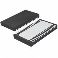
LTC4269CDKD-1#PBF Linear Technology, LTC4269CDKD-1#PBF Datasheet - Page 36

LTC4269CDKD-1#PBF
Manufacturer Part Number
LTC4269CDKD-1#PBF
Description
IC PD/OPTO FLYBACK CTRLR 32-DFN
Manufacturer
Linear Technology
Type
Power Over Ethernet (PoE)r
Datasheet
1.LTC4269IDKD-1PBF.pdf
(44 pages)
Specifications of LTC4269CDKD-1#PBF
Applications
Power Interface Switch for Power Over Ethernet (PoE) Devices
Voltage - Supply
14 V ~ 16 V
Operating Temperature
0°C ~ 70°C
Mounting Type
Surface Mount
Package / Case
32-DFN
Current - Supply
1.35mA
Interface
IEEE 802.3af
Controller Type
Powered Device Interface Controller (PD)
Input Voltage
60V
Supply Current
6.4mA
Digital Ic Case Style
DFN
No. Of Pins
32
Duty Cycle (%)
88%
Frequency
100kHz
Operating Temperature Range
0°C To +70°C
Msl
MSL 1 - Unlimited
Rohs Compliant
Yes
Operating Temperature (max)
70C
Operating Temperature (min)
0C
Pin Count
32
Mounting
Surface Mount
Package Type
DFN EP
Case Length
7mm
Screening Level
Commercial
Lead Free Status / RoHS Status
Lead free / RoHS Compliant
Available stocks
Company
Part Number
Manufacturer
Quantity
Price
LTC4269-1
The other 1% is due to the bulk C component, so use:
In many applications, the output capacitor is created from
multiple capacitors to achieve desired voltage ripple,
reliability and cost goals. For example, a low ESR ceramic
capacitor can minimize the ESR step, while an electrolytic
capacitor satisfi es the required bulk C.
Continuing our example, the output capacitor needs:
These electrical characteristics require paralleling several
low ESR capacitors possibly of mixed type.
One way to reduce cost and improve output ripple is to use a
simple LC fi lter. Figure 18 shows an example of the fi lter.
The design of the fi lter is beyond the scope of this data
sheet. However, as a starting point, use these general
guidelines. Start with a C
solution. Make C1 1/4 of C
pole independent of C
with multiple ceramic capacitors. Make L1 smaller than
the output inductance of the transformer. In general, a
0.1μH fi lter inductor is suffi cient. Add a small ceramic
capacitor (C
those interested in more details refer to “Second-Stage
LC Filter Design,” Ridley, Switching Power Magazine, July
2000 p8-10.
Circuit simulation is a way to optimize output capacitance
and fi lters, just make sure to include the component
parasitic. LTC SwitcherCAD
simulation tool that is available at www.linear.com. Final
APPLICATIONS INFORMATION
36
ESR
C
C
OUT
OUT
SECONDARY
COUT
WINDING
≥
≥
FROM
1% • V
1% • 5 • 200kHz
OUT2
≤ 1% •
5.3A
) for high frequency noise on V
I
+
OUT
OUT
5V • 1− 49.4%
L1, 0.1μH
C1
47μF
3
• f
OUT
Figure 18.
OSC
(
OUT
+
. C1 may be best implemented
5.3A
OUT
= 600µF
TM
1/4 the size of the nonfi lter
C
470μF
OUT
to make the second fi lter
is a terrifi c free circuit
)
V
= 4mΩ
OUT
C
1μF
OUT2
42691 F18
R
LOAD
OUT
. For
optimization of output ripple must be done on a dedicated
PC board. Parasitic inductance due to poor layout can
signifi cantly impact ripple. Refer to the PC Board Layout
section for more details.
ELECTRO STATIC DISCHARGE AND SURGE
PROTECTION
The LTC4269-1 is specifi ed to operate with an absolute
maximum voltage of –100V and is designed to tolerate
brief overvoltage events. However, the pins that interface
to the outside world (primarily V
can routinely see peak voltages in excess of 10kV. To
protect the LTC4269-1, it is highly recommended that the
SMAJ58A unidirectional 58V transient voltage suppressor
be installed between the diode bridge and the LTC4269-1
(D3 in Figure 2).
ISOLATION
The 802.3 standard requires Ethernet ports to be electrically
isolated from all other conductors that are user accessible.
This includes the metal chassis, other connectors and
any auxiliary power connection. For PDs, there are two
common methods to meet the isolation requirement. If
there will be any user accessible connection to the PD,
then an isolated DC/DC converter is necessary to meet
the isolation requirements. If user connections can be
avoided, then it is possible to meet the safety requirement
by completely enclosing the PD in an insulated housing.
In all PD applications, there should be no user accessible
electrical connections to the LTC4269-1 or support circuitry
other than the RJ-45 port.
LAYOUT CONSIDERATIONS FOR THE LTC4269-1
The LTC4269-1’s PD front end is relatively immune to
layout problems. Excessive parasitic capacitance on the
R
to which the exposed pad on the bottom of the package
can be soldered. This heat sink should be electrically
connected to GND. For optimum thermal performance,
make the heat sink as large as possible. Voltages in a
PD can be as large as 57V for PoE applications, so high
voltage layout techniques should be employed. The SHDN
SwitcherCAD is a trademark of Linear Technology Corporation.
CLASS
pin should be avoided. Include a PCB heat sink
PORTN
and V
PORTP
42691fb
)


