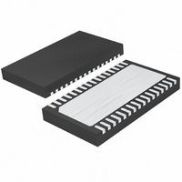
LTC4269CDKD-1#PBF Linear Technology, LTC4269CDKD-1#PBF Datasheet - Page 25

LTC4269CDKD-1#PBF
Manufacturer Part Number
LTC4269CDKD-1#PBF
Description
IC PD/OPTO FLYBACK CTRLR 32-DFN
Manufacturer
Linear Technology
Type
Power Over Ethernet (PoE)r
Datasheet
1.LTC4269IDKD-1PBF.pdf
(44 pages)
Specifications of LTC4269CDKD-1#PBF
Applications
Power Interface Switch for Power Over Ethernet (PoE) Devices
Voltage - Supply
14 V ~ 16 V
Operating Temperature
0°C ~ 70°C
Mounting Type
Surface Mount
Package / Case
32-DFN
Current - Supply
1.35mA
Interface
IEEE 802.3af
Controller Type
Powered Device Interface Controller (PD)
Input Voltage
60V
Supply Current
6.4mA
Digital Ic Case Style
DFN
No. Of Pins
32
Duty Cycle (%)
88%
Frequency
100kHz
Operating Temperature Range
0°C To +70°C
Msl
MSL 1 - Unlimited
Rohs Compliant
Yes
Operating Temperature (max)
70C
Operating Temperature (min)
0C
Pin Count
32
Mounting
Surface Mount
Package Type
DFN EP
Case Length
7mm
Screening Level
Commercial
Lead Free Status / RoHS Status
Lead free / RoHS Compliant
Available stocks
Company
Part Number
Manufacturer
Quantity
Price
APPLICATIONS INFORMATION
Note the use of the external feedback resistive divider
ratio to set output voltage provides the user additional
freedom in selecting a suitable transformer turns ratio.
Turns ratios that are the simple ratios of small integers;
e.g., 1:1, 2:1, 3:2 help facilitate transformer construction
and improve performance.
When building a supply with multiple outputs derived
through a multiple winding transformer, lower duty cycle
can improve cross regulation by keeping the synchronous
rectifi er on longer, and thus, keep secondary windings
coupled longer. For a multiple output transformer, the turns
ratio between output windings is critical and affects the
accuracy of the voltages. The ratio between two output
voltages is set with the formula V
N21 is the turns ratio between the two windings. Also
keep the secondary MOSFET R
cross regulation.
The feedback winding usually provides both the feedback
voltage and power for the LTC4269-1. Set the turns ratio
between the output and feedback winding to provide a
rectifi ed voltage that under worst-case conditions is greater
than the 11V maximum V
Leakage Inductance
Transformer leakage inductance (on either the primary or
secondary) causes a spike after the primary-side switch
turn-off. This is increasingly prominent at higher load
currents, where more stored energy is dissipated. Higher
fl yback voltage may break down the MOSFET switch if it
has too low a BV
One solution to reducing this spike is to use a clamp circuit
to suppress the voltage excursion. However, suppressing
the voltage extends the fl yback pulse width. If the fl yback
For our example: N
where:
We will choose
N
V
F
SF
= Diode Forward Voltage
>
11+ V
V
OUT
DSS
F
3
1
rating.
SF
CC
>
11+ 0.7
turn-off voltage.
5
OUT2
DS(ON)
=
= V
2.34
small to improve
OUT1
1
• N21 where
pulse extends beyond the enable delay time, output
voltage regulation is affected. The feedback system has a
deliberately limited input range, roughly ±50mV referred
to the FB node. This rejects higher voltage leakage spikes
because once a leakage spike is several volts in amplitude,
a further increase in amplitude has little effect on the
feedback system. Therefore, it is advisable to arrange the
clamp circuit to clamp at as high a voltage as possible,
observing MOSFET breakdown, such that leakage spike
duration is as short as possible. Application Note 19
provides a good reference on clamp design.
As a rough guide, leakage inductance of several percent
(of mutual inductance) or less may require a clamp, but
exhibit little to no regulation error due to leakage spike
behavior. Inductances from several percent up to, perhaps,
ten percent, cause increasing regulation error.
Avoid double digit percentage leakage inductances. There
is a potential for abrupt loss of control at high load current.
This curious condition potentially occurs when the leakage
spike becomes such a large portion of the fl yback waveform
that the processing circuitry is fooled into thinking that the
leakage spike itself is the real fl yback signal!
It then reverts to a potentially stable state whereby the
top of the leakage spike is the control point, and the
trailing edge of the leakage spike triggers the collapse
detect circuitry. This typically reduces the output voltage
abruptly to a fraction, roughly one-third to two-thirds of
its correct value.
Once load current is reduced suffi ciently, the system snaps
back to normal operation. When using transformers with
considerable leakage inductance, exercise this worst-case
check for potential bistability:
1. Operate the prototype supply at maximum expected
2. Temporarily short-circuit the output.
3. Observe that normal operation is restored.
If the output voltage is found to hang up at an abnormally
low value, the system has a problem. This is usually evident
by simultaneously viewing the primary-side MOSFET drain
voltage to observe fi rsthand the leakage spike behavior.
load current.
LTC4269-1
25
42691fb


