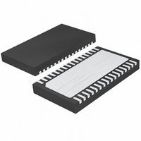
LTC4269CDKD-1#PBF Linear Technology, LTC4269CDKD-1#PBF Datasheet - Page 31

LTC4269CDKD-1#PBF
Manufacturer Part Number
LTC4269CDKD-1#PBF
Description
IC PD/OPTO FLYBACK CTRLR 32-DFN
Manufacturer
Linear Technology
Type
Power Over Ethernet (PoE)r
Datasheet
1.LTC4269IDKD-1PBF.pdf
(44 pages)
Specifications of LTC4269CDKD-1#PBF
Applications
Power Interface Switch for Power Over Ethernet (PoE) Devices
Voltage - Supply
14 V ~ 16 V
Operating Temperature
0°C ~ 70°C
Mounting Type
Surface Mount
Package / Case
32-DFN
Current - Supply
1.35mA
Interface
IEEE 802.3af
Controller Type
Powered Device Interface Controller (PD)
Input Voltage
60V
Supply Current
6.4mA
Digital Ic Case Style
DFN
No. Of Pins
32
Duty Cycle (%)
88%
Frequency
100kHz
Operating Temperature Range
0°C To +70°C
Msl
MSL 1 - Unlimited
Rohs Compliant
Yes
Operating Temperature (max)
70C
Operating Temperature (min)
0C
Pin Count
32
Mounting
Surface Mount
Package Type
DFN EP
Case Length
7mm
Screening Level
Commercial
Lead Free Status / RoHS Status
Lead free / RoHS Compliant
Available stocks
Company
Part Number
Manufacturer
Quantity
Price
APPLICATIONS INFORMATION
If we wanted a V
(5%) of hysteresis (on at 36V, off at 34.2V):
Even with good board layout, board noise may cause
problems with UVLO. You can fi lter the divider but keep
large capacitance off the UVLO node because it will slow
the hysteresis produced from the change in bias current.
Figure 13c shows an alternate method of fi ltering by split-
ting the R
more of the resistance on the UVLO side.
Converter Start-Up
The standard topology for the LTC4269-1 utilizes a third
transformer winding on the primary side that provides
both feedback information and local V
LTC4269-1 (see Figure 14). This power bootstrapping
improves converter effi ciency but is not inherently self-
starting. Start-up is affected with an external “trickle charge”
resistor and the LTC4269-1’s internal V
lockout circuit. The V
hysteresis to facilitate start-up.
In operation, the trickle charge resistor, R
to V
of 1mA to charge C
draws only its start-up current. When C
turn-on threshold voltage the LTC4269-1 turns on abruptly
and draws its normal supply current.
Switching action commences and the converter begins to
deliver power to the output. Initially the output voltage is
low and the fl yback voltage is also low, so C
most of the LTC4269-1 current (only a fraction comes
from R
some time (typically tens of milliseconds) the output
voltage approaches its desired value. The fl yback winding
then provides the LTC4269-1 supply current and the V
voltage stabilizes.
R
R
IN
B
A
=
and supplies a small current, typically on the order
=
TR
⎛
⎝ ⎜
3.4µA
1.8V
A
.) V
1.23V
resistor with the capacitor. The split should put
36V
523k
CC
= 529k, use 523k
– 1
voltage continues to drop until, after
IN
-referred trip point of 36V, with 1.8V
⎞
⎠ ⎟
TR
= 18.5k, use 18.7k
CC
. Initially the LTC4269-1 is off and
undervoltage lockout has wide
TR
CC
CC
TR
reaches the V
power for the
, is connected
undervoltage
TR
supplies
CC
CC
If C
before stabilization and the LTC4269-1 turns off. The V
node then begins to charge back up via R
threshold, where the part again turns on. Depending upon
the circuit, this may result in either several on-off cycles
before proper operation is reached, or permanent relaxation
oscillation at the V
R
current greater than the maximum rated LTC4269-1 start-up
current, and a worst-case maximum charging current less
than the minimum rated LTC4269-1 supply current.
Make C
behavior described above. This is complicated to deter-
mine theoretically as it depends on the particulars of the
secondary circuit and load behavior. Empirical testing is
recommended. Note that the use of the optional soft-start
function lengthens the power-up timing and requires a
correspondingly larger value for C
TR
R
R
and
TR
is selected to yield a worst-case minimum charging
TR(MAX)
TR(MIN)
is undersized, V
TR
+
V
IN
V
Figure 14. Typical Power Bootstrapping
large enough to avoid the relaxation oscillatory
CC(ON)
R
TR
C
TR
>
<
V
THRESHOLD
V
IN(MAX)
IN(MIN)
CC
LTC4269-1
V
I
V
VCC
VCC
I
CC
GND
V
PG
node.
CC(ST _ MAX)
0
CC
I
CC(MIN)
reaches the V
− V
− V
I
VCC
CC(ON _ MAX)
CC(ON _ MIN)
PG
V
TR
IN
LTC4269-1
CC
.
42691 F14
•
•
turn-off threshold
TR
•
to the turn-on
31
42691fb
CC


