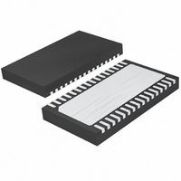
LTC4269CDKD-1#PBF Linear Technology, LTC4269CDKD-1#PBF Datasheet - Page 34

LTC4269CDKD-1#PBF
Manufacturer Part Number
LTC4269CDKD-1#PBF
Description
IC PD/OPTO FLYBACK CTRLR 32-DFN
Manufacturer
Linear Technology
Type
Power Over Ethernet (PoE)r
Datasheet
1.LTC4269IDKD-1PBF.pdf
(44 pages)
Specifications of LTC4269CDKD-1#PBF
Applications
Power Interface Switch for Power Over Ethernet (PoE) Devices
Voltage - Supply
14 V ~ 16 V
Operating Temperature
0°C ~ 70°C
Mounting Type
Surface Mount
Package / Case
32-DFN
Current - Supply
1.35mA
Interface
IEEE 802.3af
Controller Type
Powered Device Interface Controller (PD)
Input Voltage
60V
Supply Current
6.4mA
Digital Ic Case Style
DFN
No. Of Pins
32
Duty Cycle (%)
88%
Frequency
100kHz
Operating Temperature Range
0°C To +70°C
Msl
MSL 1 - Unlimited
Rohs Compliant
Yes
Operating Temperature (max)
70C
Operating Temperature (min)
0C
Pin Count
32
Mounting
Surface Mount
Package Type
DFN EP
Case Length
7mm
Screening Level
Commercial
Lead Free Status / RoHS Status
Lead free / RoHS Compliant
Available stocks
Company
Part Number
Manufacturer
Quantity
Price
APPLICATIONS INFORMATION
LTC4269-1
For each secondary-side power MOSFET, the BV
be greater than:
Choose the primary-side MOSFET R
gate drive voltage (7.5V). The secondary-side MOSFET gate
drive voltage depends on the gate drive method.
Primary-side power MOSFET RMS current is given by:
For each secondary-side power MOSFET RMS current is
given by:
Calculate MOSFET power dissipation next. Because the
primary-side power MOSFET operates at high V
transition power loss term is included for accuracy. C
is the most critical parameter in determining the transition
loss, but is not directly specifi ed on the data sheets.
C
on most MOSFET data sheets (Figure 16).
The fl at portion of the curve is the result of the Miller (gate
to-drain) capacitance as the drain voltage drops. The Miller
capacitance is computed as:
The curve is done for a given V
for different V
computed C
the curve specifi ed V
34
MILLER
BV
I
I
C
RMS(PRI)
RMS(SEC)
MILLER
DSS
is calculated from the gate charge curve included
≥ V
=
MILLER
=
=
OUT
DS
Q
V
V
Figure 16. Gate Charge Curve
B
IN(MIN)
GS
voltages are estimated by multiplying the
V
1− DC
+ V
− Q
DS
I
by the ratio of the application V
OUT
Q
IN(MAX)
a
DS
A
A
GATE CHARGE (Q
P
MILLER EFFECT
IN
MAX
.
DC
MAX
• N
DS
SP
G
Q
b
. The Miller capacitance
)
B
DS(ON)
42691 F16
at the nominal
DSS
should
MILLER
DS
DS
, a
to
With C
MOSFET power dissipation:
where:
(1 + δ) is generally given for a MOSFET in the form of a
normalized R
have a curve, use δ = 0.005/°C • ΔT for low voltage
MOSFETs.
The secondary-side power MOSFETs typically operate
at substantially lower V
losses. The dissipation is calculated using:
With power dissipation known, the MOSFETs’ junction
temperatures are obtained from the equation:
where T
junction to ambient thermal resistance.
Once you have T
δ and power dissipations until convergence.
Gate Drive Node Consideration
The PG and SG gate drivers are strong drives to minimize
gate drive rise and fall times. This improves effi ciency,
but the high frequency components of these signals can
cause problems. Keep the traces short and wide to reduce
parasitic inductance.
The parasitic inductance creates an LC tank with the
MOSFET gate capacitance. In less than ideal layouts, a
series resistance of 5Ω or more may help to dampen the
ringing at the expense of slightly slower rise and fall times
and poorer effi ciency.
R
V
f
V
P
T
P
V
OSC
TH
J
GATE(MAX)
DIS(SEC)
D(PRI)
DR
IN(MAX)
= T
MILLER
is the MOSFET gate threshold voltage
is the gate driver resistance (≈10Ω)
is the operating frequency
A
A
is the ambient temperature and θ
=I
+ P
•
= I
RMS(PRI)
determined, calculate the primary-side power
P
DS(ON)
DIS
= 7.5V for this part
DC
IN(MAX)
RMS(SEC)
J
• θ
MIN
iterate your calculations recomputing
JA
vs temperature curve. If you don’t
2
• R
• R
DS
2
• R
DS(ON)
DR
, so you can neglect transition
DS(ON)
•
V
GATE(MAX)
(
1+ δ
(1 + δ)
C
MILLER
)
+
JA
− V
is the MOSFET
TH
• f
OSC
42691fb


