DS2141A Maxim Integrated Products, DS2141A Datasheet
DS2141A
Specifications of DS2141A
Available stocks


Related parts for DS2141A

DS2141A Summary of contents
Page 1
... Isolation Stik, and DS2291 T1 Long Loop Stik DESCRIPTION The DS2141A is a comprehensive, software-driven T1 framer meant to act as a slave or coprocessor to a microcontroller or microprocessor. Quick access via the parallel control port allows a single micro to handle many T1 lines. The DS2141A is very flexible and can be configured into numerous orientations via software ...
Page 2
... This information will be used by the rest of the receive side circuitry. The DS2141A is an “off-line” framer, which means that all of the T1 serial stream that goes into the device will come out of it unchanged. Once the T1 data has been framed to, the robbed-bit signaling data and FDL can be extracted ...
Page 3
... DS2141A FEATURES Parallel control port Large error counters Onboard dual 2-frame elastic store FDL support circuitry Robbed-bit signaling extraction and insertion Programmable output clocks Fully independent transmit and receive sections Frame sync generation Error-tolerant yellow and blue alarm detection Output pin test mode ...
Page 4
... Status Register 2. Active low, open drain output. Receive Alarm Interrupt 1. Flags host controller during alarm conditions defined in Status Register 1. Active low, open drain output. Transmit Link Clock. 4 kHz or 2 kHz (ZBTSI) demand clock for the TLINK input. See Section 13 for timing details DS2141A ...
Page 5
... Z-bit position (ZBTSI). See Section 13 for timing details. Transmit Sync. A pulse at this pin will establish either frame or multiframe boundaries for the DS2141A. Via TCR2.2, the DS2141A can be programmed to output either a frame or multiframe pulse at this pin. If this pin is set to output pulses at frame boundaries, it can also be set via TCR2 ...
Page 6
... Addresses must be valid prior to the falling edge of ALE(AS), at which time the DS2141A latches the address from the AD0 to AD7 pins. Valid write data must be present and held stable during ...
Page 7
... FPS and verify with CRC6. Sync Time. 0=qualify 10 bits. 1=qualify 24 bits. Sync Enable. 0=auto resync enabled. 1=auto resync disabled. Resync. When toggled from low to high, a resync is initiated. Must be cleared and set again for a subsequent resync DS2141A (LSB) SYNCE RESYNC ...
Page 8
... S-bit position of frame 12. Fs-Bit Error Report Enable. 0=do not report bit errors in the Fs-bit position in FECR. 1=report bit errors in the Fs-bit position in FECR. BPVCRS Function Select. 0=counts bipolar violations. 1=counts ESF error events (CRC6 OR 'ed with RLOS DS2141A (LSB) FSBE BPVCRS ...
Page 9
... FDL or Fs bits from TFDL register. 1=source FDL or Fs bits from the TLINK pin. Transmit Blue Alarm. 0=transmit data normally. 1=transmit an unframed all 1's code at TPOS and TNEG. Transmit Yellow Alarm. 0=do not transmit yellow alarm. 1=transmit yellow alarm DS2141A (LSB) TBL TYEL ...
Page 10
... Section 13). TSYNC I/O Select. 0=TSYNC is an input. 1=TSYNC is an output. Transmit Side D4 Yellow Alarm Select. 0=0s in bit 2 of all channels. 1 the S-bit position of frame 12. Bit 7 Zero Suppression Enable. 0=no stuffing occurs. 1=Bit 7 forced channels with all 0s DS2141A (LSB) TD4YM B7ZS ...
Page 11
... CCR1.0 PAYLOAD LOOPBACK When CCR1.1 is set the DS2141A will be forced into Payload LoopBack (PLB). Normally, this loopback is only enabled when ESF framing is being performed PLB situation, the DS2141A will loop the 192 bits of payload data (with BPVs corrected) from the receive section back to the transmit section ...
Page 12
... LOCAL LOOPBACK When CCR1.0 is set the DS2141A will enter a Local LoopBack (LLB) mode. This loopback is useful in testing and debugging applications. In LLB, the DS2141A will loop data from the transmit side back to the receive side. This loopback is synonymous with replacing the RCLK input with the TCLK signal, and the RPOS/RNEG inputs with the TPOS/TNEG outputs ...
Page 13
... The user will always precede a read of these registers with a write. The byte written to the register will inform the DS2141A which bits the user wishes to read and have cleared. The user will write a byte to one of these three registers, with the bit positions he or she wishes to read and the bit positions he or she does not wish to obtain the latest information on ...
Page 14
... B8ZS Code Word Detect. Set when a B8ZS code word is detected at RPOS and RNEG independent of whether the B8ZS mode is selected or not via CCR2.2. Frame Bit Error. Set when a Ft (D4) or FPS (ESF) framing bit is received in error DS2141A (LSB) B8ZS FBE ...
Page 15
... Bits SR1.7 and SR1.6 will indicate when either the standard “loop up” or “loop down” codes are being received by the DS2141A. When a loop up code has been received for 5 seconds, the CPE is expected to loop the recovered data (without correcting BPVs) back to the source. The loop down code indicates that the loopback should be discontinued. See the AT& ...
Page 16
... Receive FDL Match Occurrence. Set when the RFDL matches either RFDLM1 or RFDLM2. Receive FDL Abort. Set when eight consecutive 1's are received in the FDL. Loss of Receive Clock. Set when the RCLK pin has not transitioned for at least DS2141A (LSB) RAF LORC 1 s). ...
Page 17
... Elastic Store Slip Occurrence. 0=interrupt masked. 1=interrupt enabled. Receive Blue Alarm. 0=interrupt masked. 1=interrupt enabled. Receive Yellow Alarm. 0=interrupt masked. 1=interrupt enabled. Receive Carrier Loss. 0=interrupt masked. 1=interrupt enabled. Receive Loss of Sync. 0=interrupt masked. 1=interrupt enabled DS2141A (LSB) RCL RLOS ...
Page 18
... Receive FDL Buffer Full. 0=interrupt masked. 1=interrupt enabled. Transmit FDL Buffer Empty. 0=interrupt masked. 1=interrupt enabled. Receive FDL Match Occurrence. 0=interrupt masked. 1=interrupt enabled. Receive FDL Abort. 0=interrupt masked. 1=interrupt enabled. Loss of Receive Clock. 0=interrupt masked. 1=interrupt enabled DS2141A (LSB) RAF LORC ...
Page 19
... ERROR COUNT REGISTERS There is a set of three counters in the DS2141A that record bipolar violations, errors in the CRC6 code words, and frame bit errors. Each of these three counters is automatically updated on 1-second boundaries as determined by the 1-second timer in Status Register 2 (SR2.5). Hence, these registers contain performance data from the previous second ...
Page 20
... In the receive section, the recovered FDL bits or Fs bits are shifted bit-by-bit into the Receive FDL register (RFDL). Since the RFDL is 8 bits in length, it will fill up every 250 s). The DS2141A will signal an external microcontroller that the buffer has filled via the SR2.4 bit. If enabled via IMR2.4, the INT2 pin will toggle low indicating that the buffer has filled and needs to be read ...
Page 21
... If enabled via CCR2.4, the DS2141A will automatically look for five 1 row finds such a pattern, it will automatically insert a 0 after the five 1's. The CCR2.0 bit should always be set when the DS2141A is inserting the FDL. More on how to use the DS2141A in FDL applications is covered in a separate Application Note. ...
Page 22
... The robbed bit signaling bits in embedded in the T1 stream can be extracted from the receive stream and inserted into the transmit stream by the DS2141A. There is a set of 12 registers for the receive side (RS1 to RS12) and 12 registers on the transmit side (TS1 to TS12). The signaling registers are detailed below. ...
Page 23
... SPECIAL TRANSMIT SIDE REGISTERS There is a set of seven registers in the DS2141A that can be used to custom tailor the data that transmitted onto the T1 line channel by channel basis. Each of the 24 T1 channels can be either forced to be transparent or to have a user defined idle code inserted into them. Each of these special registers is defined below ...
Page 24
... Idle Code into this DS0 channel. 1=insert the Idle Code into this channel. TIDR4 TIDR3 TIDR2 NAME AND DESCRIPTION MSB of the Idle Code. LSB of the Idle Code DS2141A (LSB) CH2 CH1 TTR1 (39) CH10 CH9 TTR2 (3A) CH18 CH17 ...
Page 25
... RCBR1.0 10.0 ELASTIC STORES OPERATION The DS2141A has two onboard two-frame (386 bits) elastic stores. These elastic stores have two main purposes. First, they can be used to rate convert the T1 data stream to 2.048 Mbps (or a multiple of 2.048 Mbps) which is the E1 rate. Secondly, they can be used to absorb the differences in frequency and phase between the T1 data stream and an asynchronous (i ...
Page 26
... The DS2141A can control line interface units that contain serial ports. When Control Register Bytes (CRB1, CRB2) are written to, the DS2141A will automatically write this data serially (LSB first) into the line interface by creating a chip select, serial clock and serial data via the LI_SDI pins respectively. This control function is driven off of the RCLK ...
Page 27
... CRB2: CONTROL REGISTER BYTE 2 (7Dh) (MSB) CR7 CR6 CR5 CR7 CR6 CR5 SYMBOL POSITION CR0 CRB1.0 CR7 CRB2.7 CR4 CR3 CR2 CR4 CR3 CR2 NAME AND DESCRIPTION LSB of Control Register Byte 1. MSB of Control Register Byte DS2141A (LSB) CR1 CR0 CRB1 (7C) CR1 CR0 CRB2 (7D) ...
Page 28
... RSYNC in the multiframe mode (RCR2.4=1). 4. ZBTSI mode disabled (RCR2.6=0). 5. RLINK data (FDL bits) is updated 1 bit time before odd frames and held for two frames. 6. ZBTSI mode is enabled (RCR2.6=1). 7. RLINK data (Z bits) is updated 1 bit time before odd frame and held for four frames DS2141A ...
Page 29
... MHz BOUNDARY TIMING (WITH ELASTIC STORE(S) ENABLED) NOTES: 1. RSER data in channels 13, 17, 21, 25, and 29 are forced to 1; TSER data in these channels will be ignored. 2. RSYNC is in the output mode (RCR2.3=0). 3. RSYNC is in the input mode (RCR2.3=1). 4. RCHBLK is forced the same channels as RSER (see Note 1 DS2141A ...
Page 30
... TSYNC in the frame mode (TCR2.3=0) and double-wide frame sync is not enabled (TCR2.4=0). 2. TSYNC in the frame mode (TCR2.3=0) and double-wide frame sync is enabled (TCR2.4=1). 3. TSYNC in the multiframe mode (TCR2.3=1). 4. TLINK data (S-bit) is sampled during the F-bit position of even frames for insertion into the outgoing T1 stream when enabled via TCR1. DS2141A ...
Page 31
... TLINK data (FDL bits) is sampled during the F-bit time of odd frame and inserted into the outgoing T1 stream if enabled via TCR1.2. 6. ZBTSI mode is enabled (TCR2.5=1). 7. TLINK data (Z bits) is sampled during the F-bit time of frame 13, 17, and 21 and inserted into the outgoing stream if enabled via TCR1. DS2141A ...
Page 32
... TSYNC is in the output mode (TCR2.2=1). 4. TCHBLK is programmed to block Channel 1. LINE INTERFACE CONTROL TIMING NOTES write to CRB1 will cause the DS2141A to output this sequence write to CRB2 will cause the DS2141A to output this sequence. 3. Timing numbers are based on RCLK=1.544 MHz with 50% duty cycle ...
Page 33
... INT1 INT2 -1.0V to +7. - +125 C 260 C for 10 seconds SYMBOL MIN TYP 4.5 DD SYMBOL MIN TYP OUT ( SYMBOL MIN TYP - 5.5V DS2141A ( MAX UNITS NOTES V +0 +0.8 V 5.5 V MAX UNITS NOTES 10%) DD MAX UNITS NOTES 10 mA +1 ...
Page 34
... Output Data Delay Time from DS or Data Setup Time ( SYMBOL MIN t 250 CYC PW 150 EL PW 100 RWH t 50 RWS DHR t 0 DHW t 20 ASL t 10 AHL t 25 ASD PW 40 ASH ASED DDR t 80 DSW DS2141A = 5V + 10%) DD TYP MAX UNITS NOTES 100 ns ns ...
Page 35
... INTEL READ AC TIMING INTEL WRITE AC TIMING MOTOROLA AC TIMING DS2141A ...
Page 36
... RPOS, RNEG, Hold from RCLK Falling RCLK Rise/Fall Times Data Delay RSYNC Setup to SYSCLK Falling RSYNC Pulse Width RECEIVE SIDE AC TIMING NOTES: 1. RSYNC is in the output mode (RCR2.3=0). 2. RSYNC is in the input mode (RCR2.3=1 SYMBOL MIN TYP MAX UNITS t 648 120 DS2141A = 5V =10%) DD NOTES ...
Page 37
... TSER, TSYNC, TLINK Setup to TCLK Falling TSER, TLINK Hold from TCLK Falling TCLK Rise/Fall Times Data Delay TSYNC Pulse Width TRANSMIT SIDE AC TIMING NOTES: 1. TSYNC is in the output mode (TCR2.2=1). 2. TSYNC is in the input mode (TCR2.2=0 SYMBOL MIN TYP MAX UNITS t 648 DS2141A = 5V + 10%) DD NOTES ...
Page 38
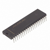
... DS2141A T1 CONTROLLER (600-MIL) 40-PIN DIP INCHES DIM MIN MAX A 2.040 2.070 B 0.530 0.560 C 0.145 0.155 D 0.600 0.625 E 0.015 0.040 F 0.120 0.140 G 0.090 0.110 H 0.625 0.675 J 0.008 0.012 K 0.015 0.022 DS2141A ...
Page 39
... DS2141AQ T1 CONTROLLER 44-PIN PLCC NOTE1: PIN 1 IDENTIFIER TO BE LOCATED IN ZONE INDICATED. INCHES DIM MIN MAX A 0.165 0.180 A1 0.090 0.120 A2 0.020 - B 0.026 0.033 B1 0.013 0.021 C 0.009 0.012 CH1 0.042 0.048 D 0.685 0.695 D1 0.650 0.656 D2 0.590 0.630 E 0.685 0.695 E1 0.650 0.656 E2 0.590 0.630 e1 0 ...