NJU3713G NJR, NJU3713G Datasheet
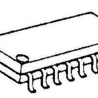
DC/DC Switching Converters 12bit Srial to Prll

NJU3713G

Manufacturer Part Number
NJU3713G
Description
DC/DC Switching Converters 12bit Srial to Prll
Manufacturer
NJR
Datasheet

Specifications of NJU3713G

Output Voltage
2.4 V to 5.5 V
Mounting Style
SMD/SMT
Package / Case
SOP-18
Operating Temperature Range
- 25 C to + 85 C
Lead Free Status / Rohs Status
Lead free / RoHS Compliant

Available stocks

Company
Part Number
Manufacturer
Quantity
Price
Part Number:
NJU3713G
Manufacturer:
JRC
Quantity:
112
Part Number:
NJU3713G(TE1)
Manufacturer:
JRC
Quantity:
20 000
Part Number:
NJU3713G-T1
Manufacturer:
JRC
Quantity:
2 000
Part Number:
NJU3713G-T1
Manufacturer:
JRC
Quantity:
1 000
Part Number:
NJU3713G-T1
Manufacturer:
JRC
Quantity:
20 000
Part Number:
NJU3713G-TE2
Manufacturer:
JRC
Quantity:
972
Part Number:
NJU3713G��TE1��
Manufacturer:
JRC
Quantity:
1 734
Ver.2003-11-18
GENERAL DESCRIPTION
especially applying to MPU outport expander.
as the connection between NJU3713 and MPU using
only 4 lines.
clock can be input to the serial data input terminal and
the data are output from parallel output buffer through
serial in parallel out shift register and parallel data
latches.
margin and the high drive-ability output buffer (25mA)
can drive LED directly.
FEATURES
BLOCK DIAGRAM
12-Bit Serial In Parallel Out
Hysteresis Input
Operating Voltage
Maximum Operating Frequency 5MHz and more
Output Current
C-MOS Technology
Package Outline
The NJU3713 is a 12-bit serial to parallel converter
The effective outport assignment of MPU is available
The serial data synchronizing with 5MHz or more
The hysteresis input circuit realizes wide noise
12-BIT SERIAL TO PARALLEL CONVERTER
DATA
CLR
CLK
STB
0.5V typ
5V±10%
25mA
DIP18/SOP18/SSOP20
Controller Circuit
P10
P11
P12
V
P5
P6
P7
P8
P9
SS
NJU3713D/G
PACKAGE OUTLINE
2
1
3
4
5
6
7
8
9
PIN CONFIGURATION
NJU3713D
18
17
16
15
14
13
12
10
11
V
P4
P3
P2
P1
CLR
STB
CLK
DATA
DD
P1
P2
P3
P11
P12
NJU3713V
P10
P12
P11
V
NC
P5
P6
P7
P8
P9
SS
NJU3713
NJU3713V
2
3
4
5
6
8
9
10
1
7
NJU3713G
20
19
18
17
16
15
14
13
12
11
- 1 -
V
P4
P3
P2
P1
NC
CLR
STB
CLK
DATA
DD

Related parts for NJU3713G

NJU3713G Summary of contents

Page 1

... Maximum Operating Frequency 5MHz and more Output Current 25mA C-MOS Technology Package Outline DIP18/SOP18/SSOP20 BLOCK DIAGRAM DATA CLK STB CLR Ver.2003-11-18 PACKAGE OUTLINE NJU3713D PIN CONFIGURATION P10 7 P11 8 P12 9 NJU3713D/G Controller Circuit NJU3713 NJU3713G NJU3713V CLR P9 STB 7 12 CLK 11 P10 8 10 ...

Page 2

NJU3713 TERMINAL DESCRIPTION No. No. SYMBOL SSOP20 DIP18/SOP18 ...

Page 3

FUNCTIONAL DESCRIPTION (1) Reset When the "L" level is input to the CLR terminal, all latches are reset and all of parallel conversion output are "L" level. Normally, the CLR terminal should be "H" level. (2) Data Transmission In the ...

Page 4

NJU3713 TIMING CHART CLK CLR STB DATA P10 P11 P12 - 4 - Ver.2003-11-18 ...

Page 5

ABSOLUTE MAXIMUM RATINGS PARAMETER Supply Voltage Range Input Voltage Range Output Voltage Range Output Current Output Short Current (P1~P12 Terminals) (Note 5) Power Dissipation (Note 6) Operating Temperature Range Storage Temperature Range Note 2) All voltage are relative to V ...

Page 6

NJU3713 SWITCHING CHARACTERISTICS PARAMETER Set-Up Time Hold Time Set-Up Time Hold Time Output Delay Time Maximum Operating Frequency Note 8) C =50pF OUT - =4.5~5.5V SYMBOL CONDITION t DATA-CLK SD t CLK-DATA HD STB-CLK t ...

Page 7

SWITCHING CHARACTERISTICS TEST WAVEFORM CLK DATA STB CLK STB P1~P12 CLK STB P1~P12 CLR DATA P1~P12 Ver.2003-11-18 f MAX HSTB t pd PSTB t pd PCLR NJU3555 NJU3555 NJU3713 t SSTB t pd PCK L ...

Page 8

NJU3713 APPLICATION CIRCUIT MPU - DATA CLK NJU3713 STB CLR P11 P10 P12 [CAUTION] The specifications on this databook are only given for information , without any guarantee as ...

Related keywords