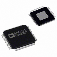
AD9852ASVZ Analog Devices Inc, AD9852ASVZ Datasheet - Page 10

AD9852ASVZ
Manufacturer Part Number
AD9852ASVZ
Description
IC DDS SYNTHESIZER CMOS 80-TQFP
Manufacturer
Analog Devices Inc
Datasheet
1.AD9852ASTZ.pdf
(52 pages)
Specifications of AD9852ASVZ
Resolution (bits)
12 b
Master Fclk
300MHz
Tuning Word Width (bits)
48 b
Voltage - Supply
3.14 V ~ 3.47 V
Operating Temperature
-40°C ~ 85°C
Mounting Type
Surface Mount
Package / Case
80-TQFP Exposed Pad, 80-eTQFP, 80-HTQFP, 80-VQFP
Transmitting Current
815mA
Rf Ic Case Style
TQFP
No. Of Pins
80
Supply Voltage Range
3.135V To 3.465V
Operating Temperature Range
-40°C To +85°C
Msl
MSL 3 - 168 Hours
Frequency Max
300MHz
Lead Free Status / RoHS Status
Lead free / RoHS Compliant
For Use With
AD9852/PCBZ - BOARD EVAL FOR AD9852
Lead Free Status / Rohs Status
Compliant
Available stocks
Company
Part Number
Manufacturer
Quantity
Price
Company:
Part Number:
AD9852ASVZ
Manufacturer:
ADI
Quantity:
263
Company:
Part Number:
AD9852ASVZ
Manufacturer:
Analog Devices Inc
Quantity:
10 000
Part Number:
AD9852ASVZ
Manufacturer:
ADI/亚德诺
Quantity:
20 000
AD9852
Pin Number
19
20
21
22
29
30
31, 32, 37, 38, 44, 50, 54,
60, 65
33, 34, 39, 40, 41, 45, 46,
47, 53, 59, 62, 66, 67
36
42
43
48
49
51
52
55
56
61
64
68
69
70
71
A0/SDIO
I/O UD CLK
FSK/BPSK/HOLD
OSK
VINN
Mnemonic
WR/SCLK
RD/CS
AVDD
AGND
VOUT
VINP
IOUT1
IOUT1
IOUT2
IOUT2
DACBP
DAC R
PLL FILTER
DIFF CLK ENABLE
REFCLK
REFCLK
S/P SELECT
MASTER RESET
SET
Description
Parallel Address Input for Program Registers (Part of 6-Bit Parallel Address Inputs for Program
Register, A5:A0)/Bidirectional Serial Data Input/Output. A0 is used only in parallel programming
mode. SDIO is used in 2-wire serial communication mode.
Bidirectional I/O Update Clock. Direction is selected in control register. If selected as an input, a
rising edge transfers the contents of the I/O port buffers to the programming registers. If I/O UD
CLK is selected as an output (default), an output pulse (low to high) with a duration of eight
system clock cycles indicates that an internal frequency update has occurred.
Write Parallel Data to I/O Port Buffers. Shared function with SCLK. Serial clock signal associated
with the serial programming bus. Data is registered on the rising edge. This pin is shared with
WR when the parallel mode is selected. The mode is dependent on Pin 70 (S/P SELECT).
Read Parallel Data from Programming Registers. Shared function with CS. Chip select signal
associated with the serial programming bus. Active low. This pin is shared with RD when the
parallel mode is selected.
Multifunction Pin. Functions according to the mode of operation selected in the programming
control register. If in the FSK mode, logic low selects F1 and logic high selects F2. If in the BPSK
mode, logic low selects Phase 1 and logic high selects Phase 2. In chirp mode, logic high
engages the hold function, causing the frequency accumulator to halt at its current location. To
resume or commence chirp, logic low is asserted.
Output Shaped Keying. Must first be selected in the programming control register to function.
A logic high causes the cosine DAC outputs to ramp up from zero-scale to full-scale amplitude
at a preprogrammed rate. Logic low causes the full-scale output to ramp down to zero scale at
the preprogrammed rate.
Connections for the Analog Circuitry Supply Voltage. Nominally 3.3 V more positive than AGND
and DGND.
Connections for Analog Circuitry Ground Return. Same potential as DGND.
Noninverted Output of the Internal High Speed Comparator. Designed to drive 10 dBm to 50 Ω
loads as well as standard CMOS logic levels.
Voltage Input Positive. The noninverting input of the internal high speed comparator.
Voltage Input Negative. The inverting input of the internal high speed comparator.
Unipolar Current Output of the Cosine DAC (refer to Figure 3).
Complementary Unipolar Current Output of the Cosine DAC.
Complementary Unipolar Current Output of the Control DAC.
Unipolar Current Output of the Control DAC.
Common Bypass Capacitor Connection for Both DACs. A 0.01 μF chip capacitor from this pin to
AVDD improves harmonic distortion and SFDR slightly. No connect is permissible, but results in
a slight degradation in SFDR.
Common Connection for Both DACs. Used to set the full-scale output current. R
Normal R
Connection for the External Zero-Compensation Network of the REFCLK Multiplier’s PLL Loop
Filter. The zero-compensation network consists of a 1.3 kΩ resistor in series with a 0.01 μF
capacitor. The other side of the network should be connected to AVDD as close as possible to
Pin 60. For optimum phase noise performance, the REFCLK multiplier can be bypassed by
setting the bypass PLL bit in Control Register 1E hex.
Differential REFCLK Enable. A high level of this pin enables the differential clock inputs, REFCLK
and REFCLK (Pin 69 and Pin 68, respectively).
Complementary (180° Out of Phase) Differential Clock Signal. User should tie this pin high or
low when single-ended clock mode is selected. Same signal levels as REFCLK.
Single-Ended (CMOS Logic Levels Required) Reference Clock Input or One of Two Differential
Clock Signals. In differential reference clock mode, both inputs can be CMOS logic levels or have
greater than 400 mV p-p square or sine waves centered about 1.6 V dc.
Selects between serial programming mode (logic low) and parallel programming mode
(logic high).
Initializes the serial/parallel programming bus to prepare for user programming, and sets
programming registers to a do-nothing state defined by the default values listed in Table 9.
Active on logic high. Asserting this pin is essential for proper operation upon power-up.
SET
range is from 8 kΩ (5 mA) to 2 kΩ (20 mA).
Rev. E | Page 10 of 52
SET
= 39.9/ I
OUT
.


