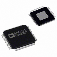
AD9852ASVZ Analog Devices Inc, AD9852ASVZ Datasheet - Page 20

AD9852ASVZ
Manufacturer Part Number
AD9852ASVZ
Description
IC DDS SYNTHESIZER CMOS 80-TQFP
Manufacturer
Analog Devices Inc
Datasheet
1.AD9852ASTZ.pdf
(52 pages)
Specifications of AD9852ASVZ
Resolution (bits)
12 b
Master Fclk
300MHz
Tuning Word Width (bits)
48 b
Voltage - Supply
3.14 V ~ 3.47 V
Operating Temperature
-40°C ~ 85°C
Mounting Type
Surface Mount
Package / Case
80-TQFP Exposed Pad, 80-eTQFP, 80-HTQFP, 80-VQFP
Transmitting Current
815mA
Rf Ic Case Style
TQFP
No. Of Pins
80
Supply Voltage Range
3.135V To 3.465V
Operating Temperature Range
-40°C To +85°C
Msl
MSL 3 - 168 Hours
Frequency Max
300MHz
Lead Free Status / RoHS Status
Lead free / RoHS Compliant
For Use With
AD9852/PCBZ - BOARD EVAL FOR AD9852
Lead Free Status / Rohs Status
Compliant
Available stocks
Company
Part Number
Manufacturer
Quantity
Price
Company:
Part Number:
AD9852ASVZ
Manufacturer:
ADI
Quantity:
263
Company:
Part Number:
AD9852ASVZ
Manufacturer:
Analog Devices Inc
Quantity:
10 000
Part Number:
AD9852ASVZ
Manufacturer:
ADI/亚德诺
Quantity:
20 000
AD9852
The purpose of ramped FSK is to provide better bandwidth
containment than can be achieved using traditional FSK. In
ramped FSK, the instantaneous frequency changes of traditional
FSK are replaced with more gradual, user-defined frequency
changes. The dwell time at F1 and F2 can be equal to or much
greater than the time spent at each intermediate frequency. The
user controls the dwell time at F1 and F2, the number of
intermediate frequencies, and the time spent at each frequency.
Unlike unramped FSK, ramped FSK requires the lowest
frequency to be loaded into the F1 registers and the highest
frequency to be loaded into the F2 registers.
Several registers must be programmed to instruct the DDS
regarding the resolution of intermediate frequency steps (48 bits)
and the time spent at each step (20 bits). Furthermore, the CLR
ACC1 bit in the control register should be toggled (low-high-low)
prior to operation to ensure that the frequency accumulator is
starting from an all 0s output condition.
FSK DATA (PIN 29)
FSK DATA (PIN 29)
I/O UD CLK
I/O UD CLK
MODE
MODE
DFW
TW1
TW2
TW1
TW2
FREQUENCY
FREQUENCY
000 (DEFAULT)
000 (DEFAULT)
F2
F1
F2
F1
0
0
0
0
0
0
Figure 34. Ramped FSK Mode (Start at F1)
Figure 35. Ramped FSK Mode (Start at F2)
REQUIRES A POSITIVE TWOS COMPLEMENT VALUE
Rev. E | Page 20 of 52
010 (RAMPED FSK)
010 (RAMPED FSK)
RAMP RATE
For piecewise, nonlinear frequency transitions, it is necessary
to reprogram the registers while the frequency transition is in
progress to affect the desired response.
Parallel Register Address 1A hex to Parallel Register Address 1C
hex comprise the 20-bit ramp rate clock registers. This is a
countdown counter that outputs a single pulse whenever the
count reaches 0. The counter is activated any time a logic level
change occurs on the FSK input (Pin 29). This counter is run at
the system clock rate, 300 MHz maximum. The time period
between each output pulse is
where N is the 20-bit ramp rate clock value programmed by
the user.
The allowable range of N is from 1 to (2
this counter clocks the 48-bit frequency accumulator shown in
F1
F2
F1
F2
(N + 1) × System Clock Period
20
− 1). The output of


