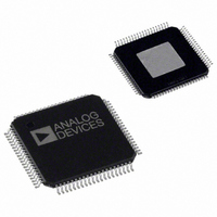
AD9852ASVZ Analog Devices Inc, AD9852ASVZ Datasheet - Page 21

AD9852ASVZ
Manufacturer Part Number
AD9852ASVZ
Description
IC DDS SYNTHESIZER CMOS 80-TQFP
Manufacturer
Analog Devices Inc
Datasheet
1.AD9852ASTZ.pdf
(52 pages)
Specifications of AD9852ASVZ
Resolution (bits)
12 b
Master Fclk
300MHz
Tuning Word Width (bits)
48 b
Voltage - Supply
3.14 V ~ 3.47 V
Operating Temperature
-40°C ~ 85°C
Mounting Type
Surface Mount
Package / Case
80-TQFP Exposed Pad, 80-eTQFP, 80-HTQFP, 80-VQFP
Transmitting Current
815mA
Rf Ic Case Style
TQFP
No. Of Pins
80
Supply Voltage Range
3.135V To 3.465V
Operating Temperature Range
-40°C To +85°C
Msl
MSL 3 - 168 Hours
Frequency Max
300MHz
Lead Free Status / RoHS Status
Lead free / RoHS Compliant
For Use With
AD9852/PCBZ - BOARD EVAL FOR AD9852
Lead Free Status / Rohs Status
Compliant
Available stocks
Company
Part Number
Manufacturer
Quantity
Price
Company:
Part Number:
AD9852ASVZ
Manufacturer:
ADI
Quantity:
263
Company:
Part Number:
AD9852ASVZ
Manufacturer:
Analog Devices Inc
Quantity:
10 000
Part Number:
AD9852ASVZ
Manufacturer:
ADI/亚德诺
Quantity:
20 000
Figure 36. The ramp rate clock determines the amount of time
spent at each intermediate frequency between F1 and F2.
The counter stops automatically when the destination
frequency is achieved. The dwell time spent at F1 and F2 is
determined by the duration that the FSK input (Pin 29) is held
high or low after the destination frequency has been reached.
Parallel Register Address 10 hex to Parallel Register Address 15 hex
comprise the 48-bit, twos complement delta frequency word
registers. This 48-bit word is accumulated (added to the
accumulator’s output) every time it receives a clock pulse from
the ramp rate counter. The output of this accumulator is added
to or subtracted from the F1 or F2 frequency word, which is
then fed into the input of the 48-bit phase accumulator that
forms the numerical phase steps for the sine and cosine wave
outputs. In this fashion, the output frequency is ramped up and
down in frequency according to the logic state of Pin 29. This
ramping rate is a function of the 20-bit ramp rate clock. When
the destination frequency is achieved, the ramp rate clock is
stopped, halting the frequency accumulation process.
Generally speaking, the delta frequency word is a much smaller
value compared with the value of the F1 or F2 tuning word. For
example, if F1 and F2 are 1 kHz apart at 13 MHz, the delta
frequency word might be only 25 Hz.
Figure 39 shows that premature toggling causes the ramp to
immediately reverse itself and proceed at the same rate and
resolution until the original frequency is reached.
The control register contains a triangle bit at Parallel Register
Address 1F hex. Setting this bit high in Mode 010 causes an
automatic ramp-up and ramp-down between F1 and F2 to
occur without toggling Pin 29 (shown in Figure 37). In fact, the
logic state of Pin 29 has no effect once the triangle bit is set
high. This function uses the ramp rate clock time period and
the step size of the delta frequency word to form a continuously
sweeping linear ramp from F1 to F2 and back to F1 with equal
dwell times at every frequency. Use this function to automatically
sweep between any two frequencies from dc to Nyquist.
In the ramped FSK mode with the triangle bit set high, an
automatic frequency sweep begins at either F1 or F2, according
to the logic level on Pin 29 (FSK input pin) when the triangle
bit’s rising edge occurs, as shown in Figure 38. If the FSK data
bit is high instead of low, F2, rather than F1, is chosen as the
start frequency.
Rev. E | Page 21 of 52
TRIANGLE BIT
TRIANGLE BIT
COMPLEMENT)
WORD (TWOS
48-BIT DELTA
FREQUENCY
I/O UD CLK
FSK DATA
FSK DATA
MODE
MODE
TW1
TW2
Figure 38. Automatic Linear Ramping Using the Triangle Bit
ACCUMULATOR
TW1
TW2
FREQUENCY
FREQUENCY
FREQUENCY
Figure 37. Effect of Triangle Bit in Ramped FSK Mode
Figure 36. Block Diagram of Ramped FSK Function
000 (DEFAULT)
RAMP RATE
CLOCK
20-BIT
0
0
F2
F1
F2
F1
0
0
FREQUENCY
TUNING
WORD 1
ADDER
010 (RAMPED FSK)
FSK (PIN 29)
FREQUENCY
ACCUMULATOR
WORD 2
TUNING
010 (RAMPED FSK)
F1
F2
PHASE
F1
F2
SYSTEM
CLOCK
INSTANTANEOUS
PHASE OUT
AD9852


