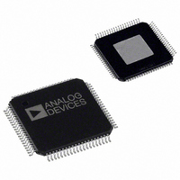
AD9852ASVZ Analog Devices Inc, AD9852ASVZ Datasheet - Page 23

AD9852ASVZ
Manufacturer Part Number
AD9852ASVZ
Description
IC DDS SYNTHESIZER CMOS 80-TQFP
Manufacturer
Analog Devices Inc
Datasheet
1.AD9852ASTZ.pdf
(52 pages)
Specifications of AD9852ASVZ
Resolution (bits)
12 b
Master Fclk
300MHz
Tuning Word Width (bits)
48 b
Voltage - Supply
3.14 V ~ 3.47 V
Operating Temperature
-40°C ~ 85°C
Mounting Type
Surface Mount
Package / Case
80-TQFP Exposed Pad, 80-eTQFP, 80-HTQFP, 80-VQFP
Transmitting Current
815mA
Rf Ic Case Style
TQFP
No. Of Pins
80
Supply Voltage Range
3.135V To 3.465V
Operating Temperature Range
-40°C To +85°C
Msl
MSL 3 - 168 Hours
Frequency Max
300MHz
Lead Free Status / RoHS Status
Lead free / RoHS Compliant
For Use With
AD9852/PCBZ - BOARD EVAL FOR AD9852
Lead Free Status / Rohs Status
Compliant
Available stocks
Company
Part Number
Manufacturer
Quantity
Price
Company:
Part Number:
AD9852ASVZ
Manufacturer:
ADI
Quantity:
263
Company:
Part Number:
AD9852ASVZ
Manufacturer:
Analog Devices Inc
Quantity:
10 000
Part Number:
AD9852ASVZ
Manufacturer:
ADI/亚德诺
Quantity:
20 000
Basic FM Chirp Programming Steps
1.
2.
3.
When programming is complete, an I/O update pulse at Pin 20
engages the program commands.
The necessity for a twos complement delta frequency word is to
define the direction in which the FM chirp moves. If the 48-bit
delta frequency word is negative (MSB is high), the incremental
frequency changes are in a negative direction from FTW1. If the
48-bit word is positive (MSB is low), the incremental frequency
changes are in a positive direction from FTW1.
Program a start frequency into Frequency Tuning Word 1
(Parallel Register Address 4 hex to Parallel Register
Address 9 hex), hereafter called FTW1.
Program the frequency step resolution into the 48-bit, twos
complement delta frequency word (Parallel Register
Address 10 hex to Parallel Register Address 15 hex).
Program the rate of change (time at each frequency) into
the 20-bit ramp rate clock (Parallel Register Address 1A hex
to Parallel Register Address 1C hex).
RAMP RATE
I/O UD CLK
MODE
DFW
TW1
FREQUENCY
000 (DEFAULT)
F1
0
0
COMPLEMENT)
WORD (TWOS
48-BIT DELTA
FREQUENCY
HOLD
ACCUMULATOR
FREQUENCY
Figure 41. Example of a Nonlinear Chirp
RAMP RATE
Figure 40. FM Chirp Components
CLOCK
20-BIT
Rev. E | Page 23 of 52
CLR ACC1
FREQUENCY
010 (RAMPED FSK)
WORD 1
TUNING
ADDER
ACCUMULATOR
It is important to note that FTW1 is only a starting point for
FM chirp. There is no built-in restraint requiring a return to
FTW1. Once the FM chirp begins, it is free to move (under
program control) within the Nyquist bandwidth (dc to one-half
the system clock). However, instant return to FTW1 can be
easily achieved.
Two control bits (CLR ACC1 and CLR ACC2) are available in the
FM chirp mode that allow the device to return to the beginning
frequency, FTW1, or to 0 Hz. When the CLR ACC1 bit (Register
Address 1F hex) is set high, the 48-bit frequency accumulator
(ACC1) output is cleared with a retriggerable one-shot pulse of
one system clock duration. The 48-bit delta frequency word input
to the accumulator is unaffected by the CLR ACC1 bit. If the
CLR ACC1 bit is held high, a one-shot pulse is delivered to the
frequency accumulator (ACC1) on every rising edge of the I/O
update clock. The effect is to interrupt the current chirp, reset the
frequency to that programmed into FTW1, and continue the chirp
at the previously programmed rate and direction. Figure 42 shows
clearing of the frequency accumulator output in chirp mode.
Shown in the diagram is the I/O update clock, which is either user
F1
PHASE
SYSTEM
CLOCK
CLR ACC2
OUT
AD9852


