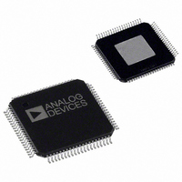
AD9852ASVZ Analog Devices Inc, AD9852ASVZ Datasheet - Page 26

AD9852ASVZ
Manufacturer Part Number
AD9852ASVZ
Description
IC DDS SYNTHESIZER CMOS 80-TQFP
Manufacturer
Analog Devices Inc
Datasheet
1.AD9852ASTZ.pdf
(52 pages)
Specifications of AD9852ASVZ
Resolution (bits)
12 b
Master Fclk
300MHz
Tuning Word Width (bits)
48 b
Voltage - Supply
3.14 V ~ 3.47 V
Operating Temperature
-40°C ~ 85°C
Mounting Type
Surface Mount
Package / Case
80-TQFP Exposed Pad, 80-eTQFP, 80-HTQFP, 80-VQFP
Transmitting Current
815mA
Rf Ic Case Style
TQFP
No. Of Pins
80
Supply Voltage Range
3.135V To 3.465V
Operating Temperature Range
-40°C To +85°C
Msl
MSL 3 - 168 Hours
Frequency Max
300MHz
Lead Free Status / RoHS Status
Lead free / RoHS Compliant
For Use With
AD9852/PCBZ - BOARD EVAL FOR AD9852
Lead Free Status / Rohs Status
Compliant
Available stocks
Company
Part Number
Manufacturer
Quantity
Price
Company:
Part Number:
AD9852ASVZ
Manufacturer:
ADI
Quantity:
263
Company:
Part Number:
AD9852ASVZ
Manufacturer:
Analog Devices Inc
Quantity:
10 000
Part Number:
AD9852ASVZ
Manufacturer:
ADI/亚德诺
Quantity:
20 000
AD9852
•
•
Continue chirp by reversing the direction and returning to
the previous or another destination frequency in a linear or
user-directed manner. If this involves reducing the
frequency, a negative 48-bit delta frequency word (the
MSB is set to 1) must be loaded into Register 10 hex to
Register 15 hex. Any decreasing frequency step of the delta
frequency word requires the MSB to be set to logic high.
Continue chirp by immediately returning to the beginning
frequency (F1) in a sawtooth fashion, and then repeating the
previous chirp process. In this case, an automatic repeating
chirp can be set up by using the 32-bit update clock to issue
the CLR ACC1 command at precise time intervals. Adjusting
the timing intervals or changing the delta frequency word
changes the chirp range. It is incumbent upon the user to
balance the chirp duration and frequency resolution to
achieve the proper frequency range.
PHASE ADJUST 1
PHASE ADJUST 2
BPSK DATA
I/O UD CLK
MODE
FTW1
000 (DEFAULT)
PHASE
360
0
0
Figure 45. BPSK Mode
Rev. E | Page 26 of 52
BPSK (MODE 100)
Binary, biphase, or bipolar phase shift keying is a means to
rapidly select between two preprogrammed 14-bit output phase
offsets. The logic state of BPSK (Pin 29) controls the selection of
Phase Adjust Register 1 or Phase Adjust Register 2. When low,
BPSK selects Phase Adjust Register 1; when high, it selects
Phase Adjust Register 2. Figure 45 illustrates phase changes
made to four cycles of an output carrier.
Basic BPSK Programming Steps
1.
2.
3.
4.
If higher-order PSK modulation is desired, the user can select
single-tone mode and program Phase Adjust Register 1 using
the serial or high speed parallel programming bus.
270°
90°
100 (BPSK)
Program a carrier frequency into Frequency Tuning Word 1.
Program the appropriate 14-bit phase words into Phase Adjust
Register 1 and Phase Adjust Register 2.
Attach the BPSK data source to Pin 29.
Activate the I/O update clock when ready.
F1


