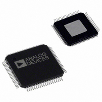
AD9852ASVZ Analog Devices Inc, AD9852ASVZ Datasheet - Page 30

AD9852ASVZ
Manufacturer Part Number
AD9852ASVZ
Description
IC DDS SYNTHESIZER CMOS 80-TQFP
Manufacturer
Analog Devices Inc
Datasheet
1.AD9852ASTZ.pdf
(52 pages)
Specifications of AD9852ASVZ
Resolution (bits)
12 b
Master Fclk
300MHz
Tuning Word Width (bits)
48 b
Voltage - Supply
3.14 V ~ 3.47 V
Operating Temperature
-40°C ~ 85°C
Mounting Type
Surface Mount
Package / Case
80-TQFP Exposed Pad, 80-eTQFP, 80-HTQFP, 80-VQFP
Transmitting Current
815mA
Rf Ic Case Style
TQFP
No. Of Pins
80
Supply Voltage Range
3.135V To 3.465V
Operating Temperature Range
-40°C To +85°C
Msl
MSL 3 - 168 Hours
Frequency Max
300MHz
Lead Free Status / RoHS Status
Lead free / RoHS Compliant
For Use With
AD9852/PCBZ - BOARD EVAL FOR AD9852
Lead Free Status / Rohs Status
Compliant
Available stocks
Company
Part Number
Manufacturer
Quantity
Price
Company:
Part Number:
AD9852ASVZ
Manufacturer:
ADI
Quantity:
263
Company:
Part Number:
AD9852ASVZ
Manufacturer:
Analog Devices Inc
Quantity:
10 000
Part Number:
AD9852ASVZ
Manufacturer:
ADI/亚德诺
Quantity:
20 000
AD9852
PLL Filter
The PLL FILTER pin (Pin 61) provides the connection for the
external zero-compensation network of the PLL loop filter. The
zero-compensation network consists of a 1.3 kΩ resistor in
series with a 0.01 μF capacitor. The other side of the network
should be connected as close as possible to Pin 60 (AVDD). For
optimum phase noise performance, the clock multiplier can be
bypassed by setting the bypass PLL bit in Control Register
Address 1E hex.
Differential REFCLK Enable
A high level on the DIFF CLK ENABLE pin enables the differential
clock inputs, REFCLK (Pin 69) and REFCLK (Pin 68). The min-
imum differential signal amplitude required is 400 mV p-p at
the REFCLK input pins. The center point or common-mode
range of the differential signal can range from 1.6 V to 1.9 V.
When Pin 64 (DIFF CLK ENABLE) is tied low, REFCLK (Pin 69)
is the only active clock input. This is referred to as single-ended
mode. In this mode, Pin 68 ( REFCLK ) should be tied low or high.
HIGH SPEED COMPARATOR
The comparator is optimized for high speed and has a toggle
rate greater than 300 MHz, low jitter, sensitive input, and built-
in hysteresis. It also has an output level of 1 V p-p minimum into
Rev. E | Page 30 of 52
50 Ω or CMOS logic levels into high impedance loads. The com-
parator can be powered down separately to conserve power. This
comparator is used in clock-generator applications to square up
the filtered sine wave generated by the DDS.
POWER-DOWN
The programming registers allow several individual stages to be
powered down to reduce power consumption while maintaining
the functionality of the desired stages. These stages are identified in
the Register Layout table (Table 9) in the Address 1D hex section.
Power-down is achieved by setting the specified bits to logic high.
A logic low indicates that the stages are powered up.
Furthermore, and perhaps most importantly, the inverse sinc
filters and the digital multiplier stages can be bypassed to achieve
significant power reduction by programming the control regis-
ters in Address 20 hex. Again, logic high causes the stage to be
bypassed. Of particular importance is the inverse sinc filter
because this stage consumes a significant amount of power.
A full power-down occurs when all four PD bits in Control
Register 1D hex are set to logic high. This reduces power
consumption to approximately 10 mW (3 mA).


