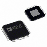
AD9852ASVZ Analog Devices Inc, AD9852ASVZ Datasheet - Page 34

AD9852ASVZ
Manufacturer Part Number
AD9852ASVZ
Description
IC DDS SYNTHESIZER CMOS 80-TQFP
Manufacturer
Analog Devices Inc
Datasheet
1.AD9852ASTZ.pdf
(52 pages)
Specifications of AD9852ASVZ
Resolution (bits)
12 b
Master Fclk
300MHz
Tuning Word Width (bits)
48 b
Voltage - Supply
3.14 V ~ 3.47 V
Operating Temperature
-40°C ~ 85°C
Mounting Type
Surface Mount
Package / Case
80-TQFP Exposed Pad, 80-eTQFP, 80-HTQFP, 80-VQFP
Transmitting Current
815mA
Rf Ic Case Style
TQFP
No. Of Pins
80
Supply Voltage Range
3.135V To 3.465V
Operating Temperature Range
-40°C To +85°C
Msl
MSL 3 - 168 Hours
Frequency Max
300MHz
Lead Free Status / RoHS Status
Lead free / RoHS Compliant
For Use With
AD9852/PCBZ - BOARD EVAL FOR AD9852
Lead Free Status / Rohs Status
Compliant
Available stocks
Company
Part Number
Manufacturer
Quantity
Price
Company:
Part Number:
AD9852ASVZ
Manufacturer:
ADI
Quantity:
263
Company:
Part Number:
AD9852ASVZ
Manufacturer:
Analog Devices Inc
Quantity:
10 000
Part Number:
AD9852ASVZ
Manufacturer:
ADI/亚德诺
Quantity:
20 000
AD9852
GENERAL OPERATION OF THE SERIAL INTERFACE
There are two phases of a serial communication cycle with the
AD9852. Phase 1 is the instruction cycle, which is the writing of
an instruction byte into the AD9852 coincident with the first
eight SCLK rising edges. The instruction byte provides the
AD9852 serial port controller with information regarding the
data transfer cycle, which is Phase 2 of the communication
cycle. The Phase 1 instruction byte defines whether the next
data transfer is a read or write and the register address to be
acted upon.
The first eight SCLK rising edges of each communication cycle
are used to write the instruction byte into the AD9852. The
remaining SCLK edges are for Phase 2 of the communication
cycle. Phase 2 is the actual data transfer between the AD9852
and the system controller. The number of data bytes transferred
during Phase 2 of the communication cycle is a function of the
register address. The AD9852 internal serial I/O controller
expects every byte of the register being accessed to be
transferred. Table 11 describes how many bytes must be
transferred.
Table 11. Register Address vs. Data Bytes Transferred
Serial
Register
Address
0
1
2
3
4
5
6
7
8
A
B
At the completion of a communication cycle, the AD9852 serial
port controller expects the subsequent eight rising SCLK edges
to be the instruction byte of the next communication cycle. In
addition, an active high input on the IO RESET pin immediately
terminates the current communication cycle. After IO RESET
returns low, the AD9852 serial port controller requires the sub-
sequent eight rising SCLK edges to be the instruction byte of
the next communication cycle.
Register Name
Phase Offset Tuning Word Register 1
Phase Offset Tuning Word Register 2
Frequency Tuning Word 1
Frequency Tuning Word 2
Delta frequency register
Update clock rate register
Ramp rate clock register
Control register
Digital multiplier register
On/off output shaped keying ramp
rate register
Control DAC register
Number
of Bytes
Transferred
2
2
6
6
6
4
3
4
2
1
2
Rev. E | Page 34 of 52
All data input to the AD9852 is registered on the rising edge of
SCLK, and all data is driven out of the AD9852 on the falling
edge of SCLK.
Figure 51 and Figure 52 are useful in understanding the general
operation of the AD9852 serial port.
INSTRUCTION BYTE
The instruction byte contains the following information:
MSB
D7
R/W
R/ W —Bit 7 of the instruction byte determines whether a read
or write data transfer occurs following the instruction byte.
Logic high indicates that a read operation will occur. Logic 0
indicates that a write operation will occur.
Bit 6, Bit 5, and Bit 4 of the instruction byte are dummy bits
(don’t care).
A3, A2, A1, A0—Bit 3, Bit 2, Bit 1, and Bit 0 of the instruction
byte determine which register is accessed during the data transfer
portion of the communication cycle (see Table 9 for register
address details).
SDIO
SDIO
SDO
CS
CS
INSTRUCTION
INSTRUCTION
INSTRUCTION
INSTRUCTION
Figure 52. Using SDIO as an Input and SDO as an Output
CYCLE
CYCLE
D6
X
BYTE
BYTE
Figure 51. Using SDIO as a Read/Write Transfer
X
D5
DATA BYTE 1
DATA BYTE 1
D4
X
DATA TRANSFER
DATA TRANSFER
DATA TRANSFER
DATA BYTE 2
DATA BYTE 2
D3
A3
D2
A2
DATA BYTE 3
DATA BYTE 3
D1
A1
LSB
D0
A0


